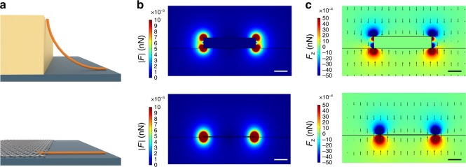
Fig. 2.
Geometrical and electrostatic conditions in graphene-based placement of nanomaterials. a Cross-section of a standard metal electrode used for electric-field-assisted assembly of nanomaterials and a graphene layer, having a thickness of 1.5 nm in our experiments, which is used for the same purpose. Both electrodes are located on top of a solid substrate. As a reference placement example, a carbon nanotube is shown that bridges contact and substrate. Cross-section of the b dielectrophoresis force distribution and c dielectrophoresis force z-component exerted on a carbon nanotube in aqueous solution which is generated by a dc voltage applied to the standard metal electrode (top) and the graphene layer (bottom), respectively. Scale bar: 50 nm

