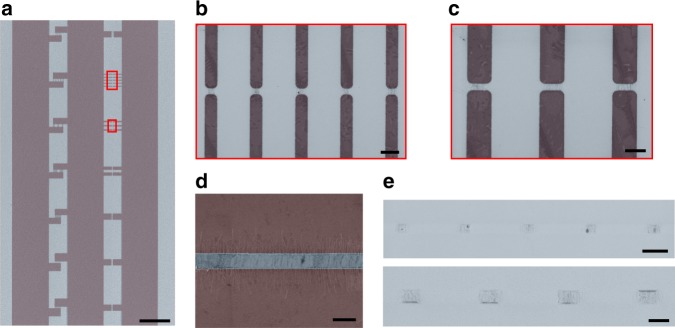
Fig. 3.
Pitch and orientation in graphene-based, electric-field-assisted nanomaterial placement. a Scanning electron microscope (SEM) false color image of a graphene layer on a SiC substrate featuring test structures of varying size and orientation for AC field-assisted assembly of carbon nanotubes from solution. The red lines frame the areas that are shown in b, c. Scale bar: 50 µm. b, c Magnified SEM false color images taken at the positions highlighted by dashed frames showing a representative graphene deposition structures after carbon nanotube placement is completed. Scale bars: 2 µm. d SEM false color image of an extended graphene electrode pair after placement is completed, exhibiting position and orientation of carbon nanotubes with respect to the gap. Scale bar: 1 µm. e SEM false color images of carbon nanotube assemblies after removal of the graphene layer leaving only CNTs and some residues. The upper panel corresponds to the area imaged in b. Scale bar: 2 µm. Deposition conditions are VDEP = 3 V, f = 1 MHz, t = 5 min

