Fig. 4.
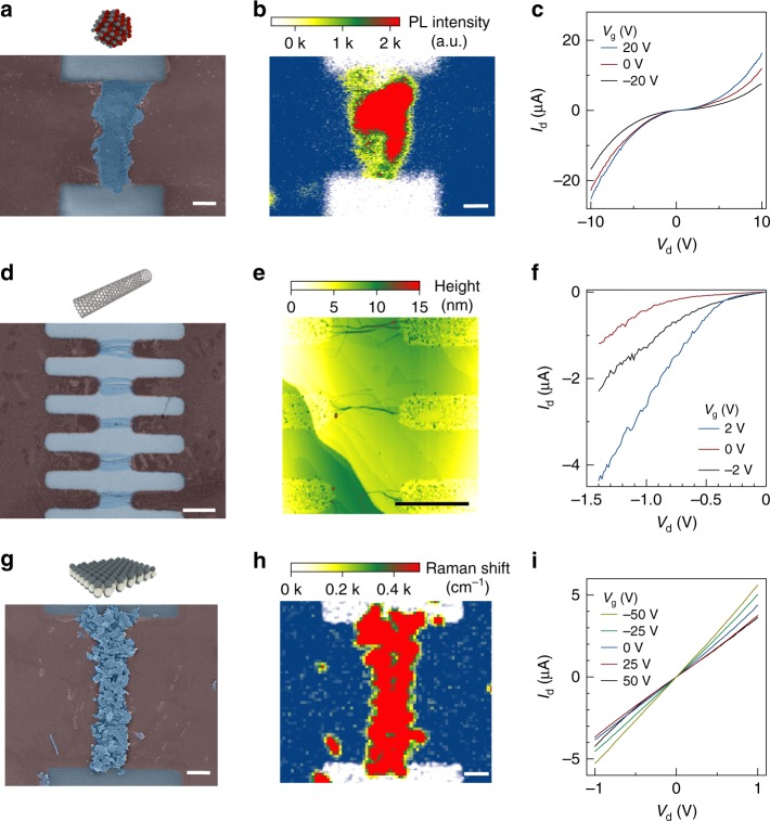
Spatially resolved deposition, characterization and device integration of 0D, 1D, and 2D semiconductors. a Scanning electron microscope (SEM) false color image of a CdSeS/ZnS quantum dot assembly. Deposition conditions are VDEP = 10 V, f = 1 MHz, t = 10 min. Scale bar: 1 µm. b Raman 2D intensity false color image (white: 20 arb. units, blue: 100 arb. units) indicating the graphene areas, overlaid by a photoluminescence intensity false color image spectrally integrated at (580 ± 10) nm indicating the position of quantum dots. The images are taken at the same area as in a. c Electrical transport characteristic of a quantum dot thin film device. Scale bar: 1 µm. d SEM false color image of carbon nanotube assembly. Deposition conditions are VDEP = 3 V, f = 1 MHz, t = 5 min. Scale bar: 1 µm. e Atomic force microscope image of the carbon nanotube assembly imaged in d. Scale bar: 1 µm. f Electrical transport characteristic of a carbon nanotube thin film device. g SEM false color image of few-layer molybdenum disulfide assembly. Deposition conditions are VDEP = 5 V, f = 1 MHz, t = 5 min. Scale bar: 1 µm. h Raman 2D intensity false color image (white: 20 arb. units, blue: 100 arb. units) indicating graphene areas, overlaid by a Raman intensity false color image spectrally integrated at (385 ± 10) cm−1 indicating the position of few-layer molybdenum disulfide. The images are taken at the same area as in g. Scale bar: 1 µm. i Electrical transport characteristic of a molybdenum disulfide thin film device

