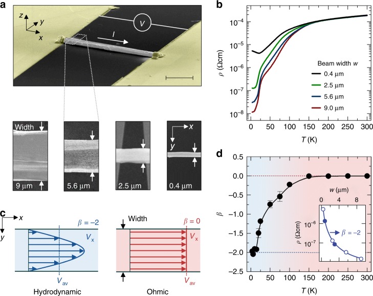
Fig. 1.
Effect of the channel width on the electrical resistivity. a False-colored scanning electron-beam microscopy (SEM) image of the device to measure the electrical resistance R = V/I (upper panel) of the WP2 micro-ribbons, where I is the applied current and V the measured voltage. x, y, and z are the spatial dimensions. The scale bar denotes 10 μm. Ribbons of four different widths w were investigated (lower panels). The error of the measured width is below 5%, including the uncertainty of the SEM and sample roughness. b Temperature (T)-dependent electrical resistivity ρ of the four ribbons. c Sketch of the velocity vx flow profile for a Stokes flow (left panel, blue line and narrows) and conventional charge flow (right panel, red line and arrows). vav is the average velocity of the charge-carrier system. β is the exponent of the functional dependence ρ(w) = ρ0 + ρ1wβ. d β as a function of T, extracted from power-law fits of the data plotted in b. The error bars denote the errors of the fits. The inset shows a power-law fit at 4 K, where the open and filled symbols represent quasi-four and four-terminal measurements, respectively. The line is a power-law fit, leading to β = −2. The colored background marks the hydrodynamic (light blue) and the normal metallic (Ohmic) temperature regime (light red)

