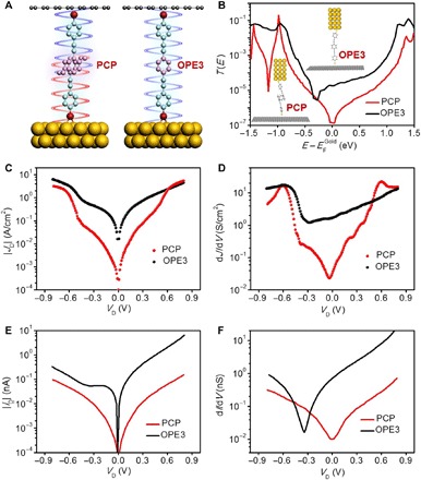
Fig. 2. Charge transport in molecular junctions.

(A) Schematic illustration of the PCP and OPE3 junctions. (B) Transmission functions T(E) for PCP (red) and OPE3 (black). Insets show the junction structures for simulation. (C) Plots of experimental current density (JD) versus bias voltage (VD) for PCP and OPE3. (D) Experimental differential conductance (dJ/dV) versus VD plots for PCP and OPE3. (E) Theoretical current (ID) versus VD plots for PCP and OPE3. (F) Theoretical differential conductance (dI/dV) versus VD plots for PCP and OPE3.
