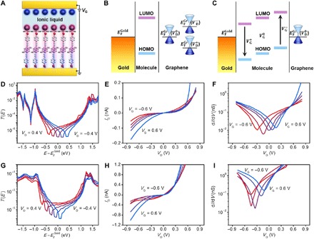
Fig. 3. Charge transport in vertical molecular transistors.

(A) Schematic illustration of the working device with EDLs. (B) Schematic band diagram of the device with changed VD at graphene electrode. (C) Schematic band diagram of the device with changed VG. (D and G) Transmission coefficient T(E) versus for PCP (D) and OPE3 (G) junctions for −0.4 < VD < 0.4 with steps of 0.2 V. (E and H) Gate-dependent theoretical ID-VD characteristics for PCP (E) and OPE3 (H). (F and I) Gate-dependent theoretical dI/dV-VD for PCP (F) and OPE3 (I). VG is varied from −0.6, −0.3, 0.0, 0.3, to 0.6 V in (E), (F), (H), and (I).
