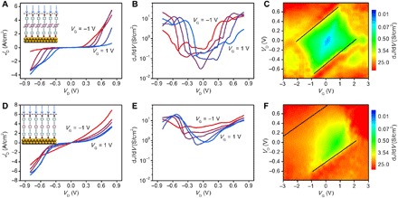
Fig. 4. Gating charge transport in experimental molecular transistors.

(A and B) JD versus VD characteristics (A) and dJ/dV versus VD characteristics (B) for PCP with VG varying from −1 to 1 V with step of 0.5 V. (C) Two-dimensional visualization of dJ/dV plotted versus VG and VD for PCP. (D and E) JD-VD characteristics (D) and dJ/dV-VD characteristics (E) for OPE3 with gating from −1 to 1 V with step of 0.5 V. (F) Two-dimensional visualization of dJ/dV plotted versus VG and VD for OPE3. Insets in (A) and (D) show schematics of the PCP and OPE3 transistors with applied vertical electric field. Black lines in (C) and (F) are auxiliary markers of corresponding conductance diamond edge.
