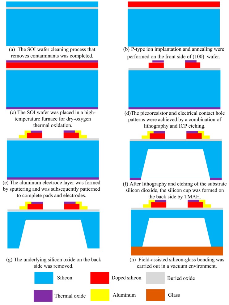
Figure 8.
Process flow of the proposed array-type piezoresistive pressure sensor (the drawing is not to scale). (a) the silicon on insulator (SOI) wafer cleaning process that removes contaminants was completed; (b) p-type ion implantation and annealing were performed on the front side of (100) SOI wafer; (c) The SOI wafer was placed in a high-temperature furnace for dry-oxygen thermal oxidation; (d) the piezoresistor and electrical contact hole patterns were achieved by a combination of lithography and ICP etching; (e) the aluminum electrode layer was formed by sputtering and was subsequently patterned to complete pads and electrodes; (f) after lithography and etching of the substrate silicon dioxide, the silicon cup was formed on the back side by tetramethylammonium hydroxide (TMAH); (g) the underlying silicon oxide on the back side was removed; (h) field-assisted silicon-glass bonding was carried out in a vacuum environment.

