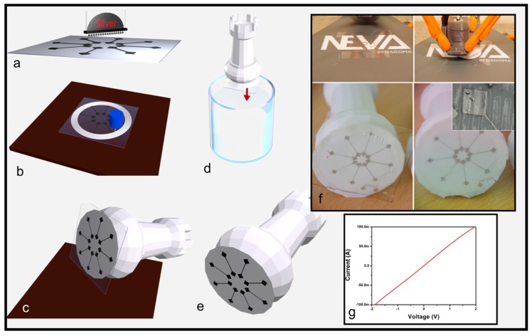
Figure 2.
Process variant used to transfer interconnects onto 3D objects additively manufactured. 3D schemes showing: (a) interconnects printed on water soluble substrate; (b) the PVA substrate is attached on the plate of the FDM equipment and the object is fabricated on top of the interconnects; (c) 3D object is detached from the plate; (d) the 3D object is dipped into a water bath; (e) PVA is dissolved and interconnects are conformally attached to the 3D object; (f) optical images showing: (i) In the first row, the PVA substrate attached to the plate (left side) and the FDM printing onto the PVA substrate (right side); (ii) in the second row, the bottom face of the 3D object after detachment of the plate but before the PVA wet etching (left side) and the final results after PVA wet etching (right side); the inset shows a zoom on a branch of the star showing conformal wrapping of the metallic patterns without mechanical failure; (g) I(V) curve.

