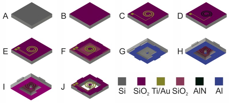
Figure 2.
Schematics of the fabrication procedure: (A) 4” Si-on-Insulator (SOI) wafer; (B) thermal oxidation (300 nm); (C) deposition and lift-off of the bottom Ti/Au contact and pads; (D) radio frequency (RF) sputter deposition and patterned etching of aluminum nitride (AlN) (830 nm); (E) deposition and lift-off of top Ti/Au contact; (F) deep reactive ion etching (DRIE) of the spiral beam from the front side; (G) first DRIE Bosch process from the back-side and the strip of the photoresist mask; (H) second DRIE Bosch process from the back-side through the Al hard mask with a slightly modified pattern to obtain perforated Si frame; (I) etching of the Al masking layer; (J) hydrofluoric acid (HF) etching of the buried oxide and removal of the top protective photoresist layer.

