Fig. 1.

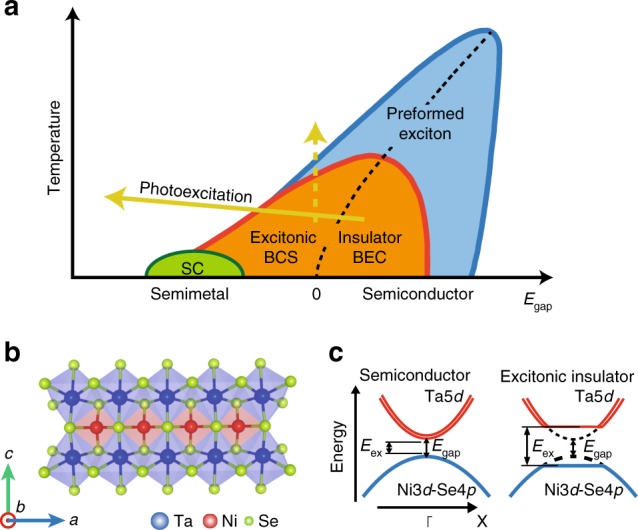
Crystal and electronic structure of Ta2NiSe5 and phase diagram of excitonic insulators. a Phase diagram of excitonic insulators. The solid arrow indicates the pathway for the photo-induced phase transition proposed in this study and the dashed arrow represents the effect of increasing the temperature. b Crystal structure of Ta2NiSe5. A quasi one-dimensional structure is formed by a single Ni chain and two Ta chains along the a-axis. c Schematic of the electronic structures of Ta2NiSe5 along the Γ–X-direction in the semiconductor and excitonic insulator phases proposed by previous studies8–11. When the exciton (which consists of an electron and a hole derived from doubly degenerate Ta 5d bands and the Ni 3d-Se 4p band) binding energy (Eex) exceeds the band gap (Egap), excitons are spontaneously formed and pure Bose–Einstein condensation of excitons arises with decreasing temperature
