Fig. 1.
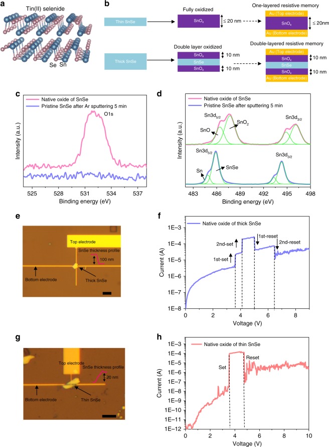
Resistive memory based on native oxide of SnSe. a Basic orthorhombic crystal structure of SnSe. b The schematic of SnSe oxidation process for two different thickness results in SnOx resistive memory and SnOx/SnSe/SnOx resistive memory. The X-ray photoelectron spectroscopy (XPS) results of native oxide of SnSe and pristine SnSe for (c) O and (d) Sn peaks. The native oxide of SnSe is the mixture of SnO2 and SnO. e The optical image and atomic force microscope (AFM) thickness profile for a 100 nm SnOx/SnSe/SnOx device. The scale bar is 5 μm. f Typical switching behavior of SnOx/SnSe/SnOx resistive memory with distinct two-step set and reset processes. g The optical image and AFM thickness profile for a 20 nm SnOx device. The scale bar is 5 μm. h Typical switching behavior of SnOx based resistive memory with regular one set and reset processes

