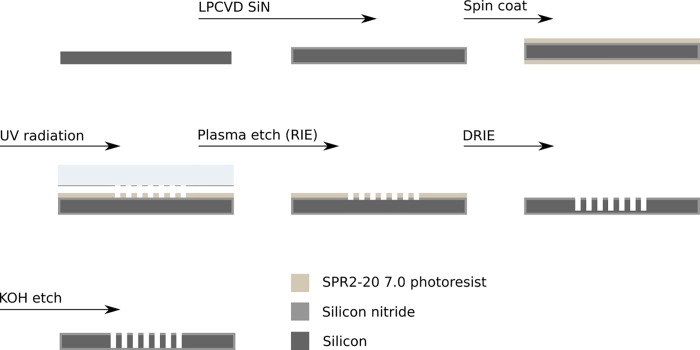
Fig 3. Overview of fabrication of silicon/silicon-nitride (Si/SiN) TEM substrates.
Wafers are initially deposited with low-stress silicon nitride (100 nm-thick) followed by photolithography, and plasma etching. In practice we fabricated eight substrates on one 100-mm diameter wafer. See Supplemental Information for fabrication plan details.

