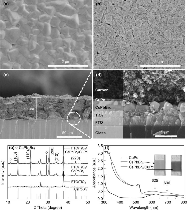
Fig. 2.

SEM images of a top view of the CsPbBr3 perovskite film and b top view of the CsPbBr3 perovskite film deposited with CuPc. c Cross-sectional SEM image of the whole device. d Close-up of the structure under higher magnification. e XRD spectra of the FTO/TiO2, FTO/TiO2/CsPbBr3, and FTO/TiO2/CsPbBr3/CuPc. f UV–Vis absorbance spectra of the CuPc, FTO/TiO2/CsPbBr3, and FTO/TiO2/CsPbBr3/CuPc
