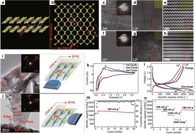
Fig. 9.
Structural characterization and electrochemical performance analysis of phosphorene electrode material in SIB: a Schematic showing the movement of Na+ ion between phosphorene layers. b Energetics dictated transport of Na+ ions in the interstices of phosphorene lattice. c, f HRTEM images along the [001] direction of few-layer phosphorene and single-layer phosphorene, respectively, with FFTs shown in the inset of each. d, g Atomic-scale high-angle annular dark field image (HAADF) along the [001] direction of few-layer phosphorene and single-layer phosphorene, respectively, with atomic orientations in inset (in yellow). e, h HAADF of few-layer phosphorene along the [100] and [010] directions, respectively, with the corresponding atomic orientations in the inset (in yellow). i, j TEM image and schematic of the contact interface of Na+ ion normal to the [100] direction and along the [100] direction, respectively. The SAED patterns of the few-layered phosphorene are shown in the inset of both. k CV of the first three cycles of the phosphorene electrode for the half cell at a scan rate of 0.005 mV s−1. l GCD profiles of the 1st, 2nd, and 30th cycle for the phosphorene electrode in the half cell. m Capacity retention and coulombic efficiency of the phosphorene electrode running at a current density of 100 mA g−1. n Rate capability of the phosphorene anode [163]. Copyright 2016 American Chemical Society. (Color figure online)

