Fig. 1.
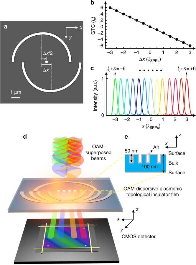
Principle of OAM nanometrology in a plasmonic topological insulator film. a The schematic design of different GTCs by shifting one half of a circular nanogroove with respect to the other along the breaking line. The GTCs are inspected in the middle of the transverse shifts (∆x/2), where ∆x is the shifting distance. b The linear dependence of the GTC (lS) on the transverse shift (∆x) of the two semi-circular nanogrooves. λSPPs represents the SPPs wavelength. c The intensity cross-sections in the transverse shift direction (the x-axis) of plasmonic fields excited by illuminating optical beams with incident angular momentum modes (l0 + s) ranging from −6 to +6 on displaced semi-circular nanogrooves with the GTCs (lS) ranging from +6 to −6, respectively. d The schematic of CMOS-integratable OAM nanometrology. An ultrathin OAM-dispersive plasmonic topological insulator film is constituted by spatially shifted semi-circular nanogrooves and mode-sorting nanoapertures, through which the OAM-superposed beams are spatially separated and directly measured by a CMOS detector in the far-field region. e The multilayer structure of the topological insulator thin film as well as the cross-section of nanogrooves

