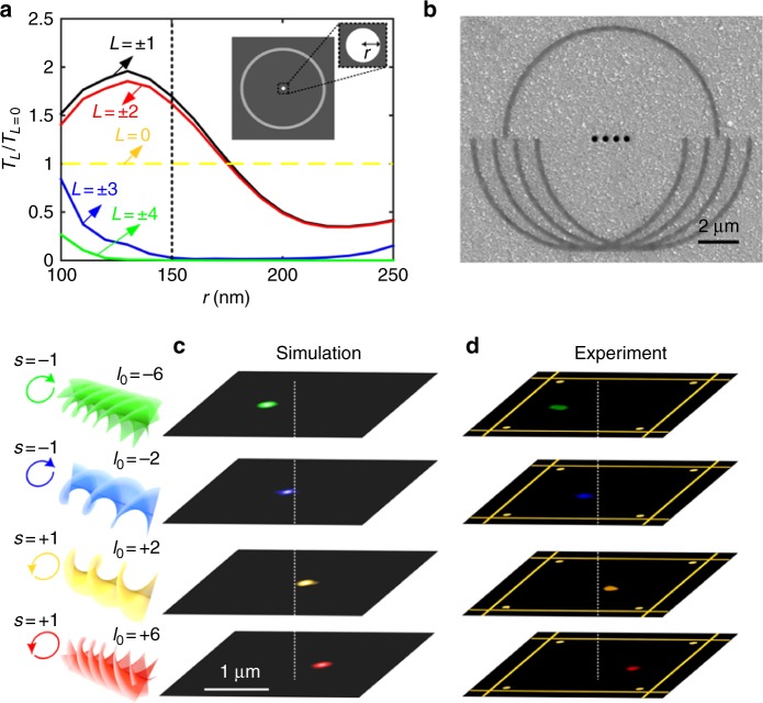
Fig. 4.
Characterization of OAM nanometrology in an ultrathin Sb2Te3 thin film. a Optical transmission of different total angular momentum modes L as a function of radius (r) of the mode-sorting nanoaperture. The transmittance curves for different angular momentum modes are normalized by the fundamental mode result with L = 0. The inset shows the schematic of the simulated nanostructures which consist of a shallow circular nanogroove and a drilled-through nanoaperture. The black dotted line labels out a mode-sorting nanoaperture waveguide with a radius of r = 150 nm used in the OAM nanometrology device. b SEM image of the fabricated four-states OAM nanometrology device. c, d Simulated (c) and experimental (d) characterization of the CMOS-integratable OAM nanometrology by inspecting the far-field transmittance patterns of the four AM modes with a spatially distinguishable shift

