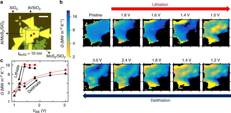
Fig. 2.
Operando scanning thermal conductance imaging. a Optical micrograph of the 10 nm thick MoS2 device. Thermal conductance images are measured within a 15 × 15 µm square region marked by the dotted lines. The scale bar is 10 µm. b Maps of the inhomogeneous thermal conductance within the device taken at different stages of lithiation and delithiation over one electrochemical cycle. These are measured after holding the MoS2 device at a constant potential VWE (relative to Li+/Li) ranging from 1.8 V to 1.0 V for discharging (lithiation) and 1.2 V to 3.0 V for charging (delithiation). c Single-point thermal conductance vs. voltage, tracked over two spots that are indicated in a by the black triangle and red square

