Fig. 4.
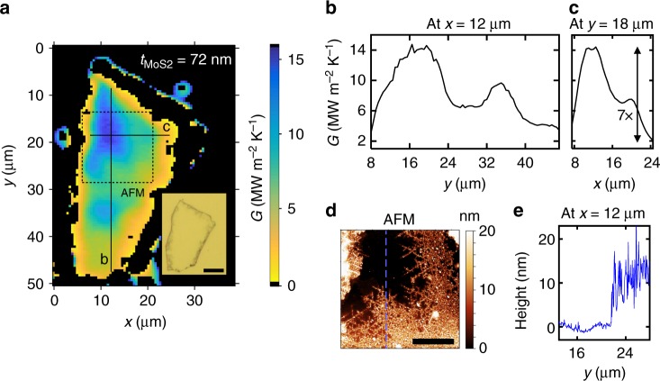
Ex situ chemical lithiation experiments. a Thermal conductance map of a 72 nm thick single crystal MoS2 film lithiated using n-Butyllithium for 2 h. Inset shows an optical micrograph of the device, after coating with 81 nm thick Al layer (scale bar is 10 µm). b Vertical line scan taken at x = 12 µm, and c horizontal line scan taken at y = 18 µm, extracted from the thermal conductance map along the solid lines marked in a. d AFM image of the region enclosed within the dashed box in a, showing a clear correlation between topography and thermal conductance. The smooth pristine region shows the highest thermal conductance, while the rough lithiated region is more thermally resistive. The scale bar is 5 µm. e Height profile extracted from the AFM image along the blue dashed line indicated in d at x = 12 µm

