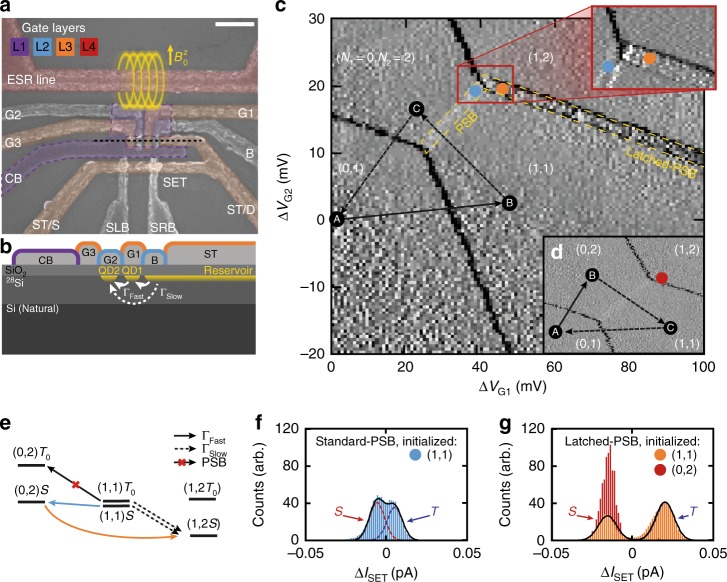
Fig. 1.
Silicon double quantum dot with latched Pauli spin blockade readout. a False-colored scanning electron micrograph of the device architecture. Dots are created under G1 and G2 electrodes and situated in the centre of the confinement gap. Scale bar is 200 nm. b Cross section illustrating dots under G1 and G2, which are tunnel-coupled with fast and slow tunnel rates ΓFast and ΓSlow to an electron reservoir under gate ST. This reservoir is located on the drain (D) side of the sensor. c Cyclic pulsing19,28 (arrows) through sequence A(0, 1)-B(1, 1)-C, where the location of point C is rastered to form the image, reveals latched spin blockade features (orange dot & top zoom-in). Shown is the differential transconductance d(ΔISET)/d(ΔVG1), where ΔISET is the difference in SET current recorded at points B and C. d When point B lies in the (0, 2) charge region, no blockade is observed, as expected for an initial singlet state. e Observation of state-latching of the G2 dot is due to weak coupling to the reservoir. In order to populate the (1, 2) state, the existing (1, 1) state must co-tunnel via (0, 2) where PSB exists. If the state is not blocked (i.e. the state) then an electron is free to tunnel from the reservoir to fill G1. Otherwise, the tunnelling from the reservoir is blocked, resulting in a spin-to-reservoir charge state conversion. f Histogram of ΔISET recorded at Standard-PSB readout location indicated by the blue marker on map d. g Histogram of ΔISET recorded at Latched-PSB readout location for B(1, 1) (orange) and B(0, 2) (red); there is a clear increase in sensitivity provided by the Latched-PSB readout

