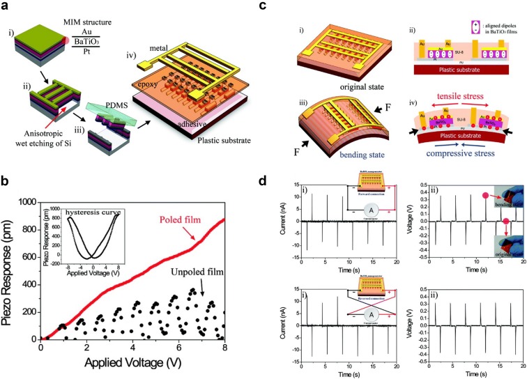
Fig. 2.
a Fabrication process of MIM structure and schematic structure of PENG with BTO thin film. b PFM measurement of BTO thin film prior to and after poling. c Deformation of BTO thin film under mechanical stress and charge induction. d Output current and voltage of PENG with fore and reverse connection
(Reproduced from [15] with copyright permission from 2010 American Chemical Society)

