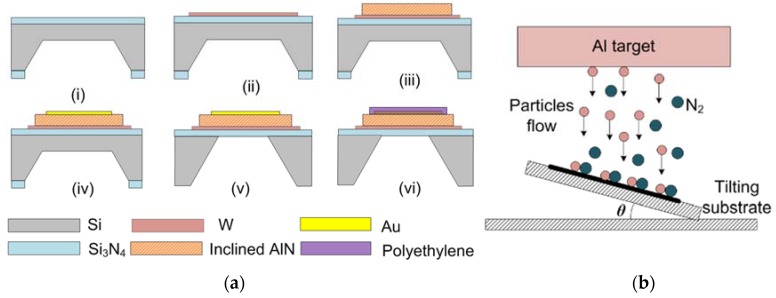
Figure 2.
(a) Fabrication process of the FBAR: (i) Etching of one side of the Si wafer with the mask of Si3N4; (ii) Deposition and pattern of bottom W electrode; (iii) Deposition and pattern of the AlN film with inclined c-axis; (iv) Preparation of top Au/Ti electrode; (v) Dry etching of the residual silicon; (vi) Spin-coating of polyethylene layer. (b) Sketch of the tilting substrate for AlN deposition (θ = 30°).

