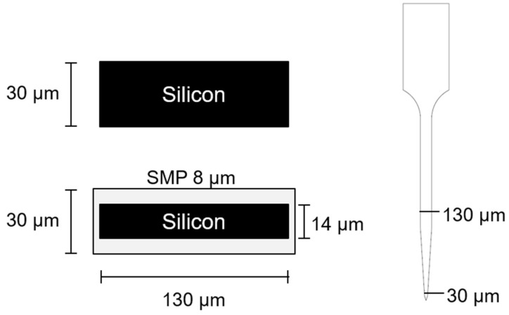
Figure 1.
Probe design schematic. Cross-sectional dimensions of the silicon (top) and dip-coated (bottom) devices and view of the profile from the side (right). Here, 30 µm thick silicon wafers were used to fabricate the bare silicon probes whereas a 14 µm thick silicon wafer (after etching) was used to produce the dip-coating substrate so that the overall device thickness resulted as ~30 µm for both device types. Due to the photomasks used, the widths of the etched silicon devices were held constant so that the bare silicon probes were 130 µm in width and after coating, the dip-coated probes were slightly larger, ~135 µm, in width. The actual coating thickness varied slightly along the length of the probe as shown in Supplementary Figure S1.

