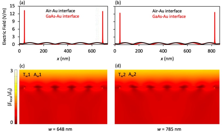
Figure 5.
(a,b) Electric field distributions on the top and the bottom interfaces of the nanostructure and (c,d) for the entire model space at Rayleigh’s anomalies as shown in Figure 3, for sweeping w. In (a) and (c), Tw1 or Aw1 is located at P = 731 nm, (w = 648 nm and g = 83 nm), and in (b) and (d), Tw2 or Aw2 is located at P = 868 nm, (w = 785 nm and g = 83 nm).

