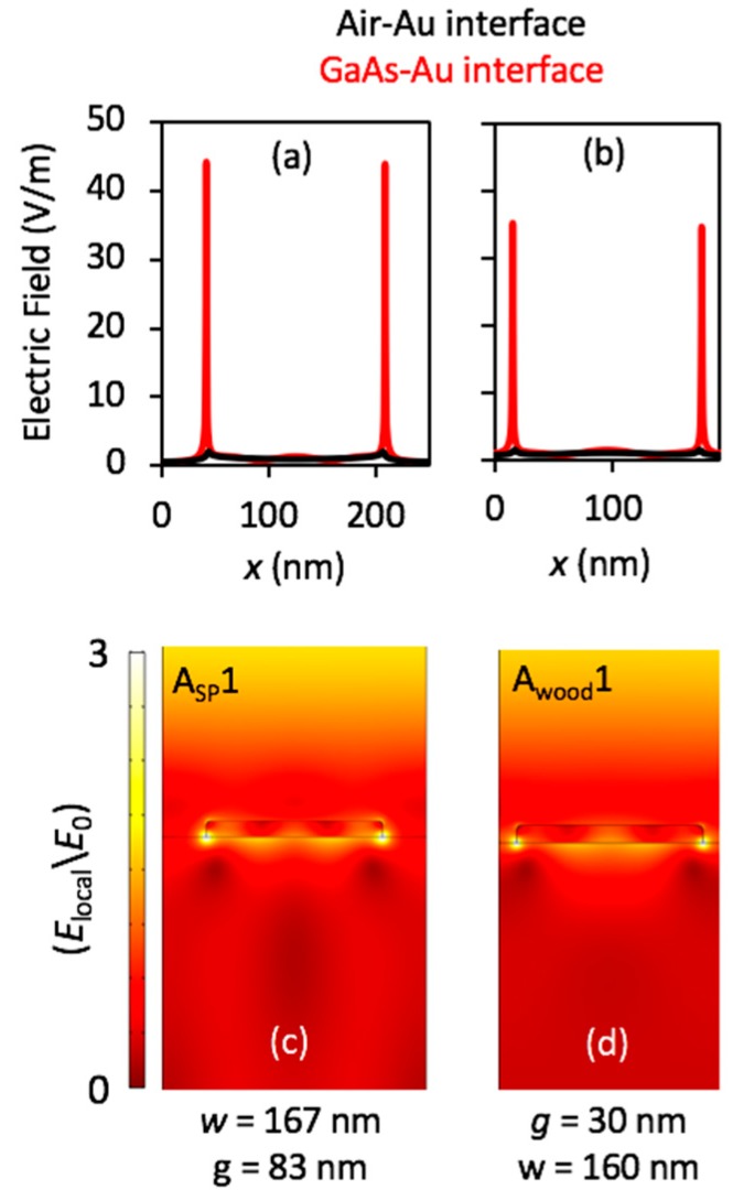
Figure 6.
(a) and (c) Asp1 and (b) and (d) Awood1 peaks as shown in Figure 3. (a,b) Electric field distributions on the top and the bottom interfaces of the nanostructure; and (c,d) over the entire model space. (a) and (c) are when P = 250 nm (w = 167 nm and g = 83 nm), and (b) and (d) when P = 190 nm (w = 160 nm and g = 30 nm).

