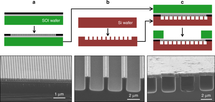
Fig. 2. Cross-sectional schematics and scanning electron microscope images of fabrication procedure.
a Pores are defined with interference lithography and etched into a silicon-on-insulator (SOI) wafer. b Microchannels are defined with projection photolithography and etched into a silicon wafer. c These two wafers are fusion bonded together and then deep reactive ion etching is used to open the back side of the SOI wafer for vapor to exit.

