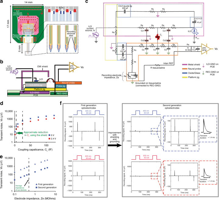
Fig. 4. Lumped circuit model to study and minimize electro magnetic interference from stimulation traces to recording traces of the assembled optoelectrode.
Front view of the assembled optoelectrode on a custom-designed PCB showing arrangement details and physical separation between ILDs, recording electrodes, ILD traces and recording traces. A representative block diagram of the optoelectrode assembly shown in a used as a reference to construct the lumped circuit model shown in c. c Lumped circuit model designed in Cadence SPICE simulator. The circuit blocks are color coded to the assembly components shown in b. The circuit was studied to minimize coupling noise from ILDs to the recording electrodes that gets picked up as high frequency transients at Intan output, VO. CL is the stray capacitance coupling from ILDs to the neural probe due to the leaky metal shield around ILD-GRIN jig assmebly. Components RS and CS in the model are parasitic resistances and capacitances of silicon and the model were simulated for 1–10 Ω of RS and 1–10 pF of CS. Ze is the impedance of electrode recording site on the neural probe and was assumed to be 500 kΩ unless Ze was the variable under study (Fig. 4e). The values of RC (contact resistance of wire bonding pads of the probe) and Rt (transmission resistance of metal interconnects on the probe) were simulated for the range of 1–100 Ω. Ri and Ci (input resistance and capacitance of Intan differential amplifier) were modeled as 65 MΩ and 12 pF, respectively, based on the product specification sheet48. The probe was assumed to be grounded in saline or tissue; which ultimately connects to the recording ground of the PCB (PCBREC-GND). Other capacitances (CILD-ILD jig; CILD jig-plat jig and CP) approximate parallel plate capacitances between different micro-fabricated silicon components. d The magnitude of stimulus-locked noise transients at VO, as a function of coupling capacitance, CL (in absence and presence of a metal shield). The reduction in CL from ~30 fF to ~5 fF with the use of an EMI metal shield proved to be successful in reducing the transients at VO to less than 100 μV. The plot also shows dependence of noise transient magnitude on ILD stimulating voltage (~5 V for 405 nm and ~2.4 V for 635 nm). Electrode impedance, Ze, is assumed as 0.5 MΩ (Re = 1.12 MΩ, Ce = 284 pF). e The magnitude of stimulation-locked transients induced by 405 nm ILD as a function of electrode impedance, Ze for first-generation optoelectrodes27 (without grounding and shielding, assumed CL = 30 fF) and second generation optoelectrodes presented in the current work (with shielding and grounding strategies implemented in the circuit model shown in (c), assumed CL = 5 fF). The current model c above shows smaller increase in transient magnitude with increase in Ze, a desirable design characteristic for chronic studies. f Reduction in transient magnitude from first generation to second generation of optoelectrodes as predicted by the circuit model. The transients reduce from 1.55 mV (for 405 nm ILD) and 0.65 mV (for 635 nm ILD) in first generation optoelectrodes to 110 μV (for 405 nm ILD) and 50 μV (for 635 nm ILD) in second generation optoelectrodes (assumed CL = 5 fF). The decay time of the transients remains the same for all cases when simulated for same values of electrode impedance (magnitude = 0.5 MΩ, phase = −65o)

