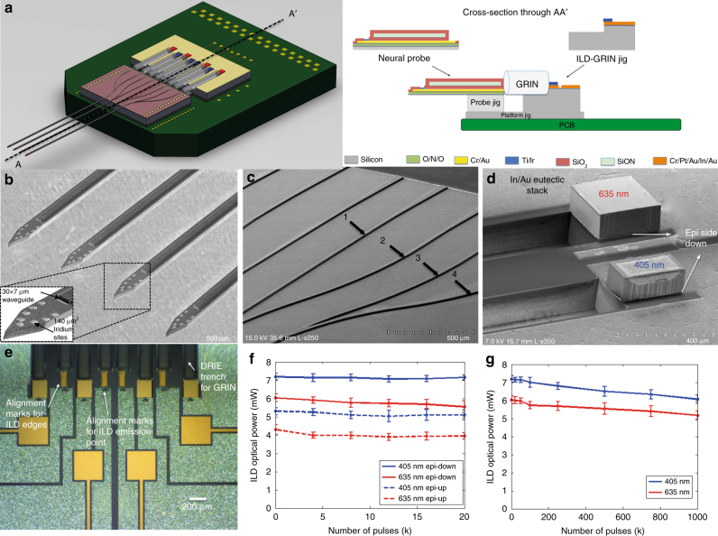
Fig. 5. Fabricated components, ILD assembly and ILD lifetime testing.
a Device fabrication details along A-A’ showing final assembly of fabricated components on PCB. The probe fabrication was carried out on a silicon-on-insulator (SOI) wafer with 22-μm thick device layer. The fabrication steps consisted of deposition of an LPCVD (low-pressure chemical vapor deposition) dielectric stack for stress compensation and electrical insulation; metal lift-off for interconnects, bondpads and electrode sites; deposition of PECVD (plasma-enhanced chemical vapor deposition)-grown waveguide (2-μm thick silicon dioxide (RI = 1.46) as bottom cladding, 7 μm thick silicon oxynitride (RI = 1.52) as core); patterning of dielectric mixer waveguides; deposition of another 2-μm thick silicon dioxide as upper cladding; contact opening for electrodes and bondpads; finally followed by probe shape definition and backside release using reactive-ion etch processes. ILD-GRIN jig fabrication started on a silicon wafer with 2-μm thick oxide for metal passivation. The process steps for the ILD-GRIN jig fabrication included lift-off of 6-μm thick indium stack to define ILD contacts and alignment marks to align ILD edges and ILD emission point; reactive-ion etching step of ~125 μm deep grooves as GRIN slots and a final dicing step to release ILD-GRIN jigs. Platform jig fabrication consisted of a single dry etch step to define shape followed by a backside release process. Probe jigs were released via dicing a wafer of a given thickness (no-mask process). b Fabricated neural probe shank tips with monolithically-integrated dielectric waveguides. The inset shows high magnification SEM image of a single shank with dielectric waveguide tip (7-μm core with 2-μm top and 2-μm bottom cladding) and iridium electrodes in Buzsaki8 configuration. c Fabricated dielectric waveguide mixer arms on the neural probe backend. All waveguide mixer arms (design 1, 2, 3, and 4) taper from 50-μm width at the backend to 30-μm width at shank tip. d High magnification SEM image of epi-side down flip-chipped 405 nm and 635 nm ILDs on the ILD-GRIN jig (heat sink made of silicon with 6 μm eutectic In/Au metal stack). e Fabricated ILD-GRIN jig (5 mm × 5 mm) with defined ILD alignment marks and eight bonded ILDs. f, g ILD characterization. f Comparison of optical power output and its decay for epi-side down and epi-side up flip-chipped ILDs (N = 5 for each ILD type, data points show the mean of the collected data and error bars represent standard deviation) when pulsed for 20,000 pulses at 5 Hz frequency, 20% duty cycle. Initial optical power of epi-side down bonded ILDs was measured to be 35.47% (for 405 nm at 30 mA) and 40.23 % (for 635 nm at 40 mA) more than that of epi-side up bonded ILDs. The optical power decay after 20,000 pulses was observed to be similar for epi-up and epi-down ILDs. g Lifetime testing of epi-down ILDs (N = 5 for each ILD type, data points show the mean of the collected data and error bars represent standard deviation) when pulsed for 1 million cycles at 5 Hz frequency, 20% duty cycle. The reduction in ILD output power after driving them through one million pulses was measured to be 18.94% for 405 nm ILDs and 16.12% for 635 nm ILDs when operated at 30 and 40 mA, respectively

