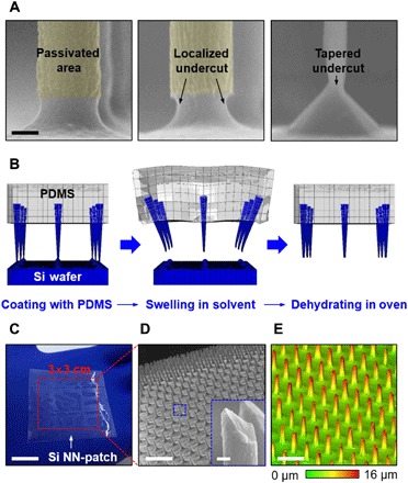
Fig. 1. Images and illustrations for the integration of vertically ordered Si NNs onto an elastomer patch.

(A) A series of scanning electron microscopy (SEM) images of vertically ordered Si pillars with selected passivation layer (left), with localized undercut (middle), and after the size is reduced down to the nanoscale (right). Scale bar, 1 μm. (B) Schematic illustrations of the key steps to physically liberate Si NNs from their native Si wafer via the swelling of PDMS. (C) Optical image of a representative Si NN-patch. Scale bar, 1.5 cm. (D) Magnified SEM image of the partly embedded Si NNs into PDMS. The inset highlights the needle-like sharp tips. Scale bars, 20 μm and 600 nm (inset). (E) Confocal laser scanning microscopy (CLSM) image of Si NNs. Scale bar, 30 μm.
