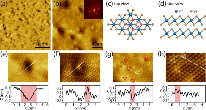
Figure 1.
(a) Large-scale STM topography image on the HfSe2 crystal (100 nm × 100 nm; It = 0.6 nA, Vs = −0.3 V). (b) Atomically resolved image of the HfSe2 surface (20 nm × 20 nm; It = 0.6 nA, Vs = −0.4 V). The inset is the corresponding fast Fourier transform image. (c) Top-view and (d) side-view sketches of a bilayer HfSe2. (e–h) Atomic-scale STM images and line scans of defects on HfSe2 (It = 0.6 nA, Vs = −0.4 V).

