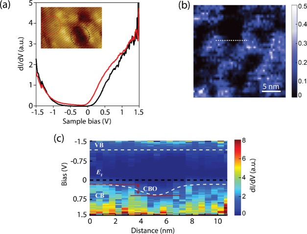
Figure 2.
Scanning tunneling spectroscopy results of the HfSe2 surface: (a) dI/dV spectra at different regions. Inset: STM image showing the locations where the spectroscopy data were taken from. (b) dI/dV map of HfSe2 (100 nm × 100 nm; It = 0.6 nA, Vs = −0.3 V). (c) Color-coded rendering of the real space imaging of the band profile plotted in terms of dI/dV taken along the dashed white line in (b).

