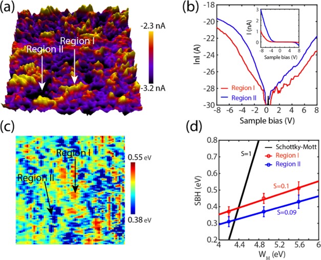
Figure 4.
(a) Current image (600 nm × 600 nm) of the HfSe2 recorded with C-AFM at a sample bias of 4.7 V. A highly doped Si tip (work function 4.2 eV) has been used. (b) Semilogarithmic contact I(V) curves for region I and region II, as indicated in panel (a). Inset: the corresponding contact I(V) curves. (c) Extracted Schottky barrier height (SBH) map (200 nm × 200 nm) of the surface extracted from I(V) curves, as shown in panel (b). The apparent SBH variations are attributed to the presence of defects on the sample. (d) The Schottky barrier heights of region I (red) and region II (blue) as a function of the tip’s work functions (Wm). The pinning factor S is extracted using eq 6. The black line refers to the standard Schottky–Mott rule (see eq 5).

