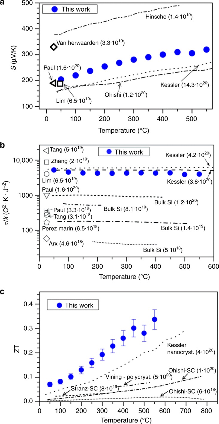
Fig. 3.

Seebeck coefficient, σ/k and figure of merit (ZT) of the fibers of nanotubes. Seebeck coefficients S as a function of the temperature T (a). The blue circles represent the fabric of this work, with nanotube wall thickness of 65 ± 5 nm. Reported values at room temperature pSi thin films with different doping levels from Paul et al.17 and Van Herwaarden et al.18 are included. Lines represent the values expected for bulk/nanobulk pSi, from Hinsche et al.19, Ohishi et al.20, and Kessler et al.22. Values in brackets indicate the boron doping concentration of the respective materials. b Geometry-independent figure σ/k as a function of temperature for the same pSi NT fabric (black squares). Values obtained from literature have been included in the graph for comparison: holey silicon nanostructures21,30, etched silicon22, thin films17,]31,32, pressed nanocristalline silicon23. c Figure of merit of the samples with different wall thickness as a function of temperature. Dash lines from bulk crystalline Si20,28 and polycristalline Si28. Dot line represents the values obtained from the work of Kessler et al.23. The main source of error reflected in the bars in the plot of ZT comes from the uncertainty in the measurement of the effective section, required for determining both σ and κ. It has been derived from the standard error of SEM cross sections obtained at different regions of the measured sample
