Figure 3.
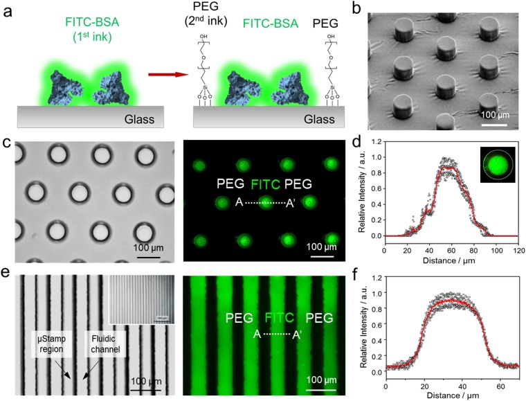
Characterization of PDMS stamp and patterned surface by μCP-DFGP. (a) Schematic representation of the sequential μCP-DFGP procedure. (b) Scanning electron micrograph of a fabricated PDMS stamp. (c) Optical image for a PDMS stamp containing a circular dot array (left) and fluorescent image of patterned FITC-BSA and surrounding PEG-silane (right). (d) Line profile showing a clearly defined bi-composite fluorescent pattern. Inset image indicates the lateral speading of patterned 1st ink. (e) Optical image for PDMS stamp containing line pattens (left) and fluorescent image for FITC-BSA/PEG-silane line patterns (right). (f) Parallel line profile showing a clearly defined bi-composite fluorescent pattern. The lines had a width of 50 μm and a spacing of 30 μm. The scale bars represent 100 μm.

