

ABSTRACT
Background: The semiconductor industry is known to use a number of chemicals, but little is known about the exact chemicals used due to the ingredients being kept as a trade secret.
Objectives: The objective of this study was to analyze chemical use using a safety data sheet (SDS) and chemical inventory provided by a major semiconductor company, which operated two factories (A and B).
Methods: Descriptive statistics were obtained on the number of chemical products and ingredients, photoresists, and carcinogens, classified by the International Agency for Research on Cancer (IARC), as well as trade secret ingredients. The total chemical use per year was estimated from chemical inventories mass (kg).
Results: A total of 428 and 432 chemical products were used in factories A and B, respectively. The number of pure chemical ingredients, after removing both trade secret ingredients and multiple counting, was 189 and 157 in factories A and B, respectively. The number of products containing carcinogens, such as sulfuric acid, catechol, and naphthalene was 47/428 (A) and 28/432 (B). Chemicals used in photolithography were 21% (A) and 26% (B) of all chemical products, and more than 97% among them were chemicals containing trade secret ingredients.
Conclusions: Each year, 4.3 and 8.3 tons of chemicals were used per person in factories A and B, respectively. Because of the high level of commercial secrecy and the use of many unregulated chemicals, more sustainable policies and methods should be implemented to address health and safety issues in the semiconductor industry.
KEYWORDS: Semiconductor, chemical, SDS, trade secret ingredients, photolithography
Introduction
The semiconductor industry, which is characterized by high levels of technological integration, has changed rapidly. A variety of chemical substances are used in the semiconductor manufacturing process. The number and amount of chemicals is increasing because of rapid technological developments in the industry [1]. Although most chemical substances used in a semiconductor manufacturing factory are known to be harmful [2–5], it is difficult to obtain hazard information for all chemicals because of the use of trade secrets. In particular, it is difficult to obtain information on the chemical content, chemical abstract service (CAS) number, ingredients, and hazards of these chemicals because of patents and trade secrets.
Workers in a semiconductor factory are likely to be exposed to carcinogens and reproductive materials [3,6–8]. In the 1980s, studies of carcinogens and chemicals used in the semiconductor industry that are harmful to workers’ reproductive health were undertaken in the US and some European countries. Health and safety issues in the semiconductor manufacturing industry have emerged since 2007 because of the onset of cancers, including leukemia, in employees who work in semiconductor manufacturing factories in Korea [9,10].
It is hard to obtain information on the number and volume of chemicals used in an actual semiconductor factory. Although there are many review papers and books documenting possible exposure to chemicals according to the processes used in the semiconductor industry, this information is generally considered to be basic and is not based on real data collected in situ. In terms of safety, health, and environmental issues, it is important to understand the actual chemical use in the semiconductor industry. The objective of this study was to analyze the chemical characteristics and chemical inventory in a large semiconductor manufacturing facility in Korea, by using a database (DB) based on safety data sheets (SDSs).
Methods
This study was conducted using a chemical information DB provided directly by a company that has a large market share of the worldwide semiconductor industry. This company has two semiconductor manufacturing factories (called A and B in this study) in Korea (Supplementary Table 1). The use of chemical substances is managed independently in each factory. The DB contains chemical information such as phase, product number, factory, product name, ingredients, CAS number, chemical content, processes used, number of units, and pattern of usage in 2014. The DB was checked using SDSs provided by the company, which also kept SDSs provided by each chemical manufacturer or supplier. Supplementary Table 2 shows part of the DB provided by the company. The phase refers to the physical status of the products supplied. Product number is the number assigned to each product at the company. The product name is the name of the actual chemical product, which sometimes contains clues regarding its chemical identity. For example, the first product name in Supplementary Table 2 contains information regarding the amount (270 kg or 448 L) of gas supplied per cylinder, while the second product name contains the term “photoresist,” which indicates that this chemical is used in photolithography. From the ingredient and CAS number column, the number of chemical ingredients and trade secrets per product, and whether a product contains any hazardous any chemicals, can be inferred. The amount of each ingredient in a product is expressed as a relative mass percentage, with a range of values provided.
The annual amount of chemicals used was calculated by using information relating to the product unit (e.g. kg, g, etc.) and statistics on usage per year. Products were purchased in a variety of units: kg, g, L, mL, gal, cylinder, bottle, and drum. Every unit was converted into a mass unit (kg or ton) using available information. For example, one cylinder of nitrous oxide has weight of 270 kg, and one bottle used in the photolithography process is 20 L. If there was no density information available, we assumed that the density was 1, so that 1 L was assumed to be 1 kg. Most of the chemical products for which no density data were available were photoresist used in the photolithography process: 84 of 428 (20%) and 153 of 432 (35%), products in factories A and B, respectively. Also, 31 of 428 (7%) and 4 of 432 (1%), products in factories A and B were excluded in the estimation of the annual amount used due to the lack of information.
In this study, when the amount of a certain ingredient used had to be calculated, the maximum value of the ingredient over the range of amounts present in a product was used. Therefore, the amounts calculated for certain ingredients could have been overestimations.
Information on health hazards, physicochemical properties, toxicity, and the Korean occupational exposure limit (OEL) was added to, or updated in the DB according to SDSs recently published by the Korea Government (http://kischem.nier.go.kr) as an integrated system for managing chemical information (as part of the Korean Occupational Safety and Health Act [Korean OSH Act], which was revised in 2015) (http://www.moel.go.kr). Carcinogens were classified according to the International Agency for Research on Cancer (IARC) classification and the Korean OSH Act.
In Supplementary Table 2, trade secret ingredients are identified in the CAS number column, and are recorded as being either resins or photosensitive compounds in the ingredients column. The trade secret ingredients were classified into six major categories according to name marked of ingredients column: additives, photoactive compounds, polymers, salts and compounds, trade secrets and others. They were further classified according to their common name, as shown in Table 5.
Table 5.
Classification of trade secret ingredients.
| No. | Description | Factory A |
Factory B |
|||
|---|---|---|---|---|---|---|
| Total† | Photoresist‡ | Total | Photoresist | |||
| 1 | Additives | 54 (16%) | 40 (20%) | 49 (13%) | 35 (13%) | |
| 2 | Photoactive compound | 42 (12%) | 39 (19%) | 63 (17%) | 58 (22%) | |
| 3 | Polymer | Resin | 40 | 28 | 56 | 36 |
| Novolac resin | 24 | 12 | 24 | 18 | ||
| Epoxy resin | 14 | 1 | 6 | 0 | ||
| Derivative | 13 | 12 | 11 | 7 | ||
| Cross-linker | 5 | 3 | 5 | 2 | ||
| Acrylate polymer | 16 | 13 | 29 | 22 | ||
| Aromatic polymer | 10 | 9 | 8 | 7 | ||
| Polymer solids | 8 | 8 | 11 | 10 | ||
| Other polymer | 15 | 7 | 8 | 5 | ||
| 145 (42%) | 93 (46%) | 158 (44%) | 107 (41%) | |||
| 4 | Salts and compounds | Organic salts and compounds | 27 | 13 | 29 | 16 |
| Inorganic salts and compounds | 20 | 0 | 2 | 0 | ||
| 47 (14%) | 13 (6%) | 31 (9%) | 16 (6%) | |||
| 5 | Trade secrets (No information) | 17 (5%) | 0 (0%) | 15 (4%) | 8 (3%) | |
| 6 | Others | Compounding chemicals | 4 | 0 | 4 | 0 |
| Monomer | 0 | 0 | 6 | 6 | ||
| Surfactant | 15 | 8 | 12 | 11 | ||
| Pigment | 0 | 0 | 12 | 12 | ||
| Others | 21 | 8 | 13 | 7 | ||
| 40 (12%) | 16 (8%) | 47 (13%) | 36 (14%) | |||
| Total | 345 (100%) | 201 (100%) | 363 (100%) | 260 (100%) | ||
† Number of ingredients (%)
‡Trade secret ingredients classified as photoresist products. The number of ingredients contained in each photoresist (%).
Results
Use of chemical products
A general overview of chemical product use in 2014 in factories A and B is provided in Table 1. The number of chemical products used in the photolithography process, which the largest number of chemicals, is presented. The number of chemical products used in factories A and B was 428 and 432, respectively. Among these, 228 (53%) were used in both factories. The total number of individual ingredients in all products was 1,136 and 1,160 in factories A and B, respectively. These figures include the multiple counting of chemical products. For example, if a chemical ingredient was contained in two products, it was recorded twice. Chemicals with a CAS number indicating that they were trade secret ingredients, and those with an unknown CAS number, were excluded. The total number of individual ingredients in all products, after multiple counting, was 788 (69%) and 780 (67%) in factories A and B, respectively. The number of pure chemical ingredients with a CAS number, without multiple counting, was 189 and 157 in factories A and B, respectively.
Table 1.
General overview of chemical products and ingredients used in 2014.
| Factory A |
Factory B |
||||||||
|---|---|---|---|---|---|---|---|---|---|
| Item | Number of products† | Number of ingredients with multiple counting‡ | Number of ingredients with a CAS No. | Average number of ingredients per product | Number of products | Number of ingredients with multiple counting | Number of ingredients with a CAS No. | Average number of ingredients per product | |
| Total | 428 (100%) | 1,136 (100%) | 189 (100%) | 2.7 | 432 (100%) | 1,160 (100%) | 157 (100%) | 2.7 | |
| Phase | Gas | 182 (43%) | 236 (21%) | 84 (44%) | 1.3 | 141 (33%) | 180 (16%) | 69 (44%) | 1.3 |
| Liquid | 221 (52%) | 781 (69%) | 96 (51%) | 3.5 | 280 (65%) | 931 (80%) | 103 (66%) | 3.3 | |
| Solid | 25 (6%) | 119 (10%) | 18 (10%) | 4.8 | 11 (3%) | 49 (4%) | 5 (3%) | 4.5 | |
| Photoresist | 92 (21%) | 398 (35%) | 37 (20%) | 4.3 | 113 (26%) | 516 (44%) | 32 (20%) | 4.6 | |
| Carcinogen* | 47 (11%) | 47 (4%) | 5 (3%) | 1.0 | 28 (6%) | 28 (2%) | 6 (4%) | 1.0 | |
†Among the total number of products, 228 were used in both factory A and B.
‡All of the chemicals, including those with trade secret ingredients and unknown CAS numbers, were counted, even if the same ingredients were contained in different products.
*Chemical name [carcinogenicity class, factory]: sulfuric acid (strong acid mist) [1A, A, and B], catechol [2B, A, and B], diborane [2B, A, and B], naphthalene [2B, A, and B], carbon black [2B, A, and B], and 1,4-dioxane [2B, B].
Most chemicals used in semiconductors are supplied in the liquid or gas phase. In factories A and B, 52% and 65% of chemical products were liquids, and 43% and 33% were in the gas phase, respectively. Only 6% and 3% were used in the solid phase in factories A and B, respectively, and most of them were epoxy molding compounds (EMCs), consisting of silica (CAS No. 60,676–86-0) and carbon black (CAS No. 1333–86-4). Gaseous chemicals were supplied as a pure gas (e.g. Ar as arsine) or, in a few cases, as a composite containing the gas (e.g. 4% phosphine in 96% helium). Liquid or solid chemical products contained more ingredients: the average number of chemical ingredients per product was 1.3 for the gas phase in factories A and B, 3.5 or 3.3 for the liquid phase, and 4.8 or 4.5 for the solid phase in factories A and B, respectively.
In the photolithography process, 21% (92) and 26% (113) of the chemical products were used in factories A and B, respectively. Of these products, 37 and 32 chemical ingredients with a CAS number were included in factories A and B. All of these chemical products, called photoresists, were present in the liquid phase, with the number of chemical ingredients per product being 4.3 and 4.6 in factories A and B, respectively. The photoresist products have more ingredients than the liquid products used in the other processes.
The chemical ingredients classified into groups 1, 2A, or 2B by the IARC, and their associated products, are presented in Table 1. Ethyl alcohol, classified into group 1, was excluded because only the drinking of alcohol was considered to pose a carcinogenic risk. The number of products with carcinogen ingredients was 47 (11%) and 28 (6%) in factories A and B, respectively. The number of ingredients when multiple counting was conducted was identical, which indicates that there was only one carcinogenic ingredient per product. Without multiple counting, only five and six ingredients were classified as carcinogens in factories A and B, respectively: sulfuric acid (CAS No. 7664–93-9), catechol (12–80-9), diborane (19,287–45-7), naphthalene (91–20-3), and carbon black (1333–86-4) in factory A, and the same five chemicals plus 1,4-dioxane (123–91-1) in factory B. Sulfuric acid was classified as a group 1 product, while the others were in group 2B.
The most frequently used chemical ingredients are listed in Table 2. In both factories, the same three chemicals were the most common ingredients: propylene glycol monomethyl ether acetate (PGMEA; CAS No. 108–65-6), cyclohexanone (108–94-1), and propylene glycol monomethyl ether (PGME; 107–98-2). PGMEA was included in 21% (92/428) of all products in factory A, and in 28% (121/432) of all products in factory B (with most of the use being for photolithography; 79% (73/92) in factory A, and 80% (90/113) in factory B). The average PGMEA content per product used in photolithography was 72% (range: 15–99%) in factory A and 68% (10–98%) in factory B. In photolithography, in addition to PGMEA, cyclohexanone, PGME, gamma-butyrolactone, and ethyl lactate were frequently used. Vitreous silica and carbon black were used in the EMCs in a packaging plant. The average EMC content per silica product was 90% (90–93%) in factory A and 91% (90–95%) in factory B, while for carbon black products it was 1% in both factories. Most of the chemical products used in the packaging plant were EMCs, which contained vitreous silica, carbon black phenol, and/or epoxy resin or lead (Pb)-free solder balls, which in turn contained silver (Ag) and tin (Sn). Some chemicals were used in two or more processes. Isopropyl alcohol and acetone are the most popular cleaning solvents in the semiconductor industry.
Table 2.
List of chemicals most frequently contained in semiconductor-manufactured products.
| Order | Factory A |
|
Factory B |
||||||
|---|---|---|---|---|---|---|---|---|---|
| Chemical name | CAS No. | Number of products (%) | Number of products used in photolithography (%) | Chemical name | CAS No. | Number of products (%) | Number of products used in photolithography (%) | ||
| 1 | Propylene glycol monomethyl ether acetate | 108–65-6 | 92 (21.5) | 73 (79.3) | Propylene glycol monomethyl ether acetate | 108–65-6 | 121 (28.0) | 90 (79.6) | |
| 2 | Cyclohexanone | 108–94-1 | 25 (5.8) | 23 (25.0) | Cyclohexanone | 108–94-1 | 44 (10.2) | 38 (33.6) | |
| 3 | Propylene glycol Monomethyl ether | 107–98-2 | 24 (5.6) | 13 (14.1) | Propylene Glycol Monomethyl Ether | 107–98-2 | 35 (8.1) | 16 (14.2) | |
| 4 | Silica, vitreous | 60,676–86-0 | 23 (5.4) | Gamma-Butyrolacton | 96–48-0 | 33 (7.6) | 24 (21.2) | ||
| 5 | Carbon black | 1333–86-4 | 21 (4.9) | Ethyl lactate | 97–64-3 | 20 (4.6) | 19 (16.8) | ||
| 6 | Gamma-butyrolacton | 96–48-0 | 20 (4.7) | 17 (18.5) | Hydrofluoric Acid | 7664–39-3 | 14 (3.2) | ||
| 7 | Sulfuric acid | 7664–93-9 | 18 (4.2) | 2-Methoxy-1-propanol | 1589–47-5 | 13 (3.0) | |||
| 8 | Ethyl lactate | 97–64-3 | 16 (3.7) | 15 (16.3) | Silica, vitreous | 60,676–86-0 | 13 (3.0) | ||
| 9 | Copper(Ⅱ) sulfate | 7758–98-7 | 15 (3.5) | Neon | 7440–01-09 | 13 (3.0) | |||
| 10 | Hydrogen | 1333–74-0 | 12 (2.8) | Carbon black | 1333–86-4 | 11 (2.5) | |||
| Total | 428 (100) | 92 (100) | Total | 432 (100) | 113 (100) | ||||
The amount of chemicals used on a mass basis is summarized in Table 3. As described in the Method section, the mass of 93% and 99% of the products in factories A and B was estimated. In total, 46,850 and 45,628 ton/year were used in factories A and B, respectively. Among these, chemicals in the liquid phase accounted for 95% (44,371 ton) and 97% (44,284 ton) of the usage in factories A and B, respectively, followed by the gas phase (3% in both factories), and solid phase (2% and 0.1% in factories A and B, respectively).
Table 3.
Amount of chemicals used (by mass and number) and chemical classification by occupational exposure limit (OEL) designation.
| Factory A |
Factory B |
||||
|---|---|---|---|---|---|
| Number | Amount (ton) | Number | Amount (ton) | ||
| Classification by phase | Gas | 180 | 1,317 | 141 | 1,303 |
| Liquid | 216 | 44,371 | 277 | 44,284 | |
| Solid | 1 | 1,163 | 10 | 40 | |
| Total | 397 | 46,850 | 428 | 45,628 | |
| Classification by OEL | OEL | 44 | 20,890 | 46 | 25,218 |
| Not listed by OEL | 140 | 23,649 | 106 | 20,849 | |
| Total | 184 | 44,539 | 152 | 46,067 | |
The number of chemical ingredients with a Korean OEL designation was 44 among 189 (23%), and 46 among 157 (29%), of the chemicals identified as ingredients, i.e. those with a CAS number, in factories A and B, respectively. In terms of mass, these figures were 47% and 55%, respectively. This means that more than 70% of the chemical ingredients in terms of number, and about half of them in terms of mass, had no OEL (including those classified as trade secrets).
Figure 1 shows the amount of chemicals classified as carcinogens by the IARC in terms of mass. In factory A, the mass of carcinogenic chemicals was estimated to be 12,816 tons, although this figure was derived from only 27 of 47 carcinogenic ingredients (with multiple counting applied, as shown in Table 1) due to the lack of information provided. Without multiple counting, only four chemicals (sulfuric acid, catechol, diborane, and naphthalene) were used to estimate the amount of carcinogens. In factory B, mass information was derived for 27 of 28 carcinogenic chemical ingredients, with a final estimate of 11,952 tons. 29% in factory A and 26% in factory B of the total mass of chemicals was carcinogenic, with sulfuric acid (CAS No. 7664–93-9; IARC carcinogen group 1) accounting for more than 99.8% of the total (12,804 tons in factory A and 11,930 tons in factory B). In this estimation, the amount of carbon black used in factory A was not considered due to the lack of information.
Figure 1.
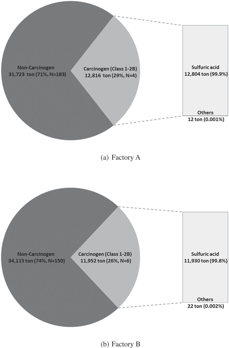
Number of chemicals classified as carcinogenic by the International Agency for Research on Cancer (IARC) in terms of mass.
Trade secret ingredients
Table 4 gives the number of products and ingredients classified as trade secrets according to the overall contents indicated in the SDSs. There were 186 (43%) and 168 (39%) products classified as trade secrets in factories A and B, respectively. When ingredients were also included, there were 345 and 363 (about 30%) materials classified as trade secrets in factories A and B, respectively.
Table 4.
The number of products and ingredients classified as trade secrets.
| Content comprising trade secret ingredients | Factory A |
|
Factory B |
||||||
|---|---|---|---|---|---|---|---|---|---|
| Product |
Ingredient |
Product |
Ingredient |
||||||
| Total | Photoresist | Total | Photoresist | Total | Photoresist | Total | Photoresist | ||
| <1% | 4 | 0 | 80 | 11 | 2 | 0 | 76 | 8 | |
| 1–30% | 147 | 74 | 209 | 172 | 127 | 81 | 241 | 226 | |
| 30–60% | 15 | 9 | 2 | 5 | 28 | 22 | 4 | 5 | |
| 60–80% | 6 | 3 | 3 | 0 | 1 | 0 | 0 | 0 | |
| >80% | 7 | 0 | 6 | 0 | 1 | 0 | 1 | 0 | |
| NI† | 7 | 4 | 45 | 13 | 9 | 7 | 41 | 21 | |
| Overall (%)‡ | 186 (43) | 90 (98) | 345 (30) | 201 (51) | 168 (39) | 110 (97) | 363 (31) | 260 (50) | |
†NI, no information available
‡percentage was calculated as the number of trade secret products or ingredients divided by the total number of products or ingredients
We found that most photoresist products contained trade secret ingredients. As shown in Table 4, 90 of 92 photoresist products (98%) in factory A, and 110 of 113 photoresist products (97%) in factory B, contained at least one trade secret ingredient. When also considering the ingredients, 51% (201 out of 398 materials) in factory A, and 50% (260 out of 516 materials) in factory B were classified as trade secrets. The average number of trade secret ingredients per product was about 0.8 in factories A (345 out of 428) and B (363 out of 432) for all products, whereas the average number was 2.2 (92 out of 201) in factory A and 2.3 (113 out of 260) in factory B for photoresist products.
Products containing trade secret ingredients were categorized by content (<1%, 1–30%, 30–60%, 60–80%, >80% trade secret ingredients). The amount of trade secret ingredients in products was largest in the ranges of 1 ~ 30% (147 out of 186 and 127 out of 168 products in factories A and B, respectively) and 30 ~ 60% (15 out of 186 and 28 out of 168 products in factories A and B, respectively). Seven products in factory A and one product in factory B were composed of more than 80% trade secret ingredients. In such cases, the product itself was sometimes marked as a trade secret as shown in Table 4.
The trade secret ingredients, categorized according to their general names, are presented in Table 5. Several types of polymer were identified as ingredients in both factory A (145 out of 345 [42%] ingredients) and factory B (158 out of 363 (44%) ingredients). This polymer category was further divided into nine sub-categories, as shown in Table 5.
In the polymer category, resins were the ingredients most frequently found in both factories, followed by novolac resin, acrylate polymer, epoxy resin, derivatives, and aromatic polymers. More than half of the novolac resin, known to consist of phenolic polymer and/or cresol, used in all processes was used in photoresist products in both factories. Most of the epoxy resin used was contained within EMCs applied in the molding process at the packaging plant. Almost all of the acrylate polymer, aromatic polymer, and polymer solids marked as polymers were used in photoresists; 30 out of 34 in factory A and 39 out of 48 in factory B. Polymers marked as “additives” accounted for 16% and 13% of all polymers in factories A and B, respectively. Photoactive compounds were typical components of photoresist products within which they were predominantly used. More than half of all organic salts were used in photoresist products, but inorganic salts and their compounds were not used in those products. Materials labeled as “trade secret,” with no common name given, accounted for about 5% of the total in both factories. Other groups of materials included surfactants, monomers, pigments, compounding chemicals, and those belonging to the category “other.”
The trade secret ingredient mass values, presented by category in Table 5, are also presented in Figure 2. There were 40.4 tons of polymers used in factory A, with 72% (29.1 tons) used in photoresist products; and there were 54.7 tons of polymers used in factory B, with 68% (37.4 tons) used in photoresist products. All of the photoactive compounds, 6.7 tons in factory A and 6.5 tons in factory B, were used in photoresist products. There were 23.1 and 19.0 tons of salts and their compounds used in factories A and B, respectively, and nearly all of them were used in non-photolithography processes. About half of the organic compounds identified were used in photolithography, as shown in Table 5.
Figure 2.
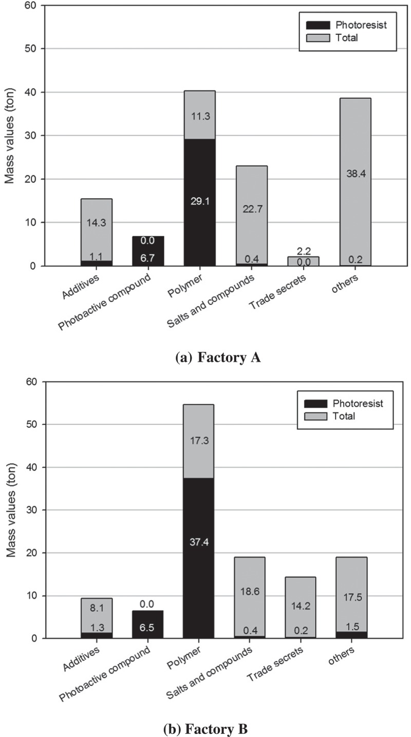
Amounts of trade secret ingredients in terms of mass by material category. (a) Factory A (b) Factory B.
Discussion
We found that more than 150 pure chemical substances were used in about 430 chemical products in a semiconductor company; about 40% of these chemical products contained trade secret ingredients. In photolithography, one of the most widely used processes in semiconductor manufacturing, nearly all products (about 98%) contained trade secret ingredients, with an average number of approximately two per product.
The amount of chemicals used was 46,850 and 45,628 tons in factories A and B, respectively, with the employees in each factory numbering approximately 110,000 and 5,500, respectively. The chemical use per person during 1 year was therefore 4.26 tons in factory A and 8.3 tons in factory B. We did not determine the exact reason for this difference in chemical use per person, but it may be due to the facility age (factory A was established in 1983, while factory B was established in 1989 [and had been frequently renovated]), final products produced (the main product in factory A was DRAM compared to NAND in factory B), or to the final amount of product produced (these data could not be obtained). It is not clear if the amount of chemical usage recorded is large or small compared to other industries, but a chemical use per person that exceeds 4.6 tons a year is considerable.
SDSs enable workers to assess the health and safety conditions in their workplace, but the large amount of trade secret ingredients used in the semiconductor manufacturing industry makes it difficult to obtain accurate health and safety information. These trade secret ingredients could easily be omitted during airborne chemical monitoring and related risk assessments, even though they may be hazardous.
We found that 40% of all products in both factories contained at least one trade secret ingredient. In 2011, a report was published claiming that 45% of chemical products in Korean chemical manufacturing plants contained at least one trade secret ingredient [11]. As shown in Table 4, more than 97% of chemicals used in the photolithography process contained trade secret ingredients, with the average number of trade secret ingredients per product being 2.3.
The trade secret ingredients shown in Table 5 were classified according to their corresponding SDSs, but some trade secret ingredients could have been included in other categories. The chemicals used in the photolithography process are classified as photoactive compounds, polymers, solvents, or additives [12,13]. Almost all of the trade secrets ingredients were photoactive compounds and polymers. Photoactive compounds that react with light generate an acid, and then the dissolution properties of the polymer are changed. For example, many polymers are used as photoactive compounds, but are classified only by their name. Six monomers identified in factory B must in fact be units of a polymer, because monomers are not usually used in the semiconductor industry. However, we classified them as monomers according to the information provided on the SDSs. Certain trade secret ingredients listed as “additive” and “trade secrets” in Table 5 could belong to the photoactive compound or polymer groups, because they were used in the photolithography process.
An understanding of the semiconductor manufacturing process is necessary to evaluate the chemical use in the industry. For example, as technology has developed, the width of the patterning line on the wafer surface has decreased and the chemicals used have changed accordingly. In the past, novolac resin was usually used as a polymer during application of spectral lines at 436 nm (“g-line”) and 365 nm (“i-line”). However, as shorter wavelengths have been developed, polyhydroxystyrene (PHS) polymer and acrylate polymer have been used instead of novolac resin to produce KrF (248 nm) and ArF (193 nm) light sources, respectively [12,14–16]. In the company investigated here, many light sources were used and therefore many polymers were also employed.
More than 97% of the products used in the photolithography process in both factories included trade secret ingredients. Therefore, it was difficult to determine the exact characteristics of the products using the SDSs of products provided by the chemicals manufacturer.
According to the Korea OSH Act, in Korea, carcinogens, mutagens, and reproductive toxins (CMRs) should be listed in SDSs if their contents are above a defined limit (≥0.1% for carcinogens and mutagens and ≥0.3% for reproductive toxins). In this study, we could not confirm the existence of CMRs or other health hazards within trade secret ingredients due to the secrecy involved, although more than 340 ingredients were categorized as trade secret ingredients, as shown in Table 5. We are now conducting a further study to analyze photoresist products and determine which are CMRs.
The photolithography process uses many chemical products, which in turn contain many organic solvents and polymers. These solvents, and the by-products of polymers, could be emitted during coating, as well as the soft bake and hard bake stages. After photoresist coating in photolithography, a wafer-coated photoresist is baked at 70–90°C in the soft bake stage, and at 120–135°C in the hard bake stage [8].
It is known that certain unused chemicals, including benzene, toluene, cresol, and other chemicals, are generated during the pyrolysis of photoresist products containing novolac resin [17]; more sensitive workers might feel uncomfortable about the attendant risk of adverse health effects [18].
During the packaging process, EMCs are representative compounds used in molding. On average, four ingredients were identified in EMCs in this study, including carbon black and silica (84% of all products in factory A and all products in factory B), as well as trade secret ingredients such as phenolic and epoxy resins. Although almost all of the EMCs were composed of silica (average 90%) and carbon black (average 1%), epoxy and/or phenolic resins were also present in EMCs and photoresist products. It was reported previously that benzene (an IARC group 1 carcinogen), phenol, and formaldehyde (an IARC group 1 carcinogen) were generated as byproducts of EMCs during the molding process, although their concentrations were low [17,19]. Pb was used as a solder ball ingredient in the past, but is no longer used because it is subject to the European Union (EU) legislation on the restriction of hazardous substances (RoHS) [20].
Although the proportion of products that included carcinogens, as classified by the IARC, was only about 10% of the total number of products used in both factories, we found that the proportion of carcinogenic ingredients was about 30% of the total amount of ingredients used. Sulfuric acid, an IARC group 1 carcinogen, accounted for more than 99% of the total amount of carcinogenic chemicals. Many studies have reported that sulfuric acid is used in a variety of semiconductor manufacturing processes, including cleaning, wet etching, and wet stripping, all of which are subsumed by the fabrication process [3,13,21]. According to the “Survey on the distribution and use of chemicals; sulfuric acid” published by the Korea Occupational Safety and Health Agency (KOSHA) in 2009, sulfuric acid with a 98% concentration has been used as a wafer etchant in the semiconductor manufacturing industry [22]. This was also apparent from the information provided on the SDS referred to in this study. In Korea, the airborne concentration of sulfuric acid in semiconductor manufacturing facilities is reported to be low or non-detectable [23].
In the company investigated here, there was no DB or management system that could be consulted to determine how many chemical products were used in each process, and in what amounts.
It was difficult to classify chemical products by process because the Safety, Health, and Environment (SHE) team in the company had no DB available that we could consult. The process of semiconductor chip manufacturing is usually divided into fabrication and packaging stages [8,24]. We could only use promotional materials provided by the company in our investigation. The fabrication process has been categorized into various photolithography stages, as follows: etching; thin film (T/F) production, including chemical vapor deposition (CVD) and physical vapor deposition (PVD); diffusion, including implanting and furnace heating (oxidation, annealing); and C&C including chemical mechanical polishing (CMP) and cleaning. In another process, metal copper was used to make a chip in both factory A and factory B. The packaging stage consists of back grinding, wafer sawing, die attachment, wire bonding, molding, marking, solder ball mounting, a saw singulation test – which includes a test during burn in (TDBI) – and packing. During fabrication, chemicals are used in every step, especially in the photolithography process. In packaging, most chemicals are used in the molding, solder ball mounting, and marking processes. Some chemicals are used in several processes, with cleaning solvents like isopropanol and acetone used both in the fabrication and packaging stages.
The Korean government frequently inspects the semiconductor company involved in this study. After the most recent survey, the company implemented a human resource management system and integrated it with a “job exposure matrix (JEM)” in which every worker’s job history, chemical use, and qualitative exposure were recorded.
It is not easy to manage levels of exposure to chemicals in the absence of guidelines or standards. In the workplace, OELs frequently used as a guideline or legal standard. As shown in Table 3, a very small proportion (24% [44/184] and 30% (46/152]) of the chemicals used in factories A and B, respectively, have OELs. The other chemicals used are not monitored or regulated. It should be noted that the chemicals used in the semiconductor industry have different characteristics compared to the chemicals used in other manufacturing industries. For example, they were introduced relatively recently, they are atypical compared to the chemicals used in other manufacturing industries, there is a high level of secrecy regarding their composition, and there has been a rapid change in the use of these chemicals following recent technological developments [5,10]. This makes it difficult to control chemical hazards in the semiconductor industry.
Trade secrets are difficult in terms of work environment management, although they are necessary for companies. Because we do not know the harmfulness of the substance without knowing the ingredient. Moreover, as shown in Table 4, many chemical products contain trade secrets and the contents of trade secrets are high in many cases. In the SDS, trade secrets are limited to the component name and content. It is important that all other information, including health and safety information, is recorded so that it is known to the user. If the name of the ingredient is not known, it can not be verified that the remaining information is correct. If the content of the trade secret substance is high, it means that the amount of the ingredient is unknown, which means that the risk increases. The SDS should contain the trade secret ingredient only if it is absolutely necessary, but if not interested in the government or the down streamer, the chemical manufacturer may set a lot of trade secrets intentionally and/or unintentionally. In Korea, preliminary trade secrets review system will be introduced to the Industrial Safety and Health Act in order to supplement these shortcomings.
This study had some limitations. First, it was difficult to estimate the exact amount of ingredients used because the content of each ingredient was provided as a range in the SDSs. We used the maximum value of the range reported in the SDSs when estimating the amount of each ingredient, but this did not affect the amount of product originally produced this company. Second, the photoresist chemicals classified by the process could not be estimated exactly, as explained in the Discussion section. Third, this study was conducted by consulting only a chemical DB and SDS. If there were any disparities between the information contained within these documents and their actual use in the workplace, there could be errors in the analysis. For example, factory A contained a research institute, in which many chemicals were used and removed on a temporary basis, but we could not locate it within the facility.
Conclusions
This study evaluated chemical use in two factories operated by one of the largest semiconductor manufacturing companies in the world. More than 420 chemical products (428 in factory A and 432 in factory B), which contained more than 150 pure chemical ingredients (189 in factory A and 157 in factory B) were used, with 40% of them containing trade secret ingredients. More than 97% of the chemical products used in the photolithography process, one of the most widely applied chemical processes, contained trade secret ingredients. Less than 30% of the chemical ingredients had OELs. Because of the high percentage of trade secret ingredients, limited number of regulated chemicals, and atypical chemical use compared to other industries, it is difficult to assess health hazards in the semiconductor industry. In 2014, more than 45,000 tons of chemicals were used in each factory and sulfuric acid, classified as a group 1 carcinogen by the IARC, accounted for about 30% of the total amount.
It is important to establish and implement a chemical management program in-house.
The company will filter out chemical components that should not be entered at the time of purchase of chemical products and establish a system to review SDS and other safety and health information to comply with laws and regulations. The company should share chemicals management policies with chemical suppliers and make efforts to reduce the number of possible trade secret substances. Periodically update the SDS of incoming chemicals with the latest information and practice the right of workers to know. It shall periodically receive a certificate that the trade secret substance does not contain substances prohibited by law, including CMR.
Funding Statement
This work was supported by the BrainKorea21 (BK21) Plus Project of the National Research Foundation (NRF) [Grant number 5280-20180100].
Acknowledgments
This work was supported by BrainKorea21 (BK21) Plus project of the National Research Foundation (NRF) [Grant number 2580-20180100].
Disclosure statement
All authors have no conflicts of interest to declare.
SUPPLEMENTAL DATA
The supplement data can be assessed here.
References
- [1].Aftalion F.The chemical revolution In: Aftalion F, editor. A history of the international chemical industry. USA: Chemical Heritage Foundation; 2001. p. 15–16. [Google Scholar]
- [2].Courtney D.Health hazards of soft soldering in the electronics industry. Rev Environ Health. 1984;5(1):1–26. [PubMed] [Google Scholar]
- [3].Chelton CF, Glowatz M, Mosovsky JA. Chemical hazards in the semiconductor industry. IEEE Trans Edu. 1991;34(3):269–288. [Google Scholar]
- [4].Harrison M. Semiconductor manufacturing hazards In: Krieger GR, editor. Hazardous materials toxicology: clinical principles of environmental health. USA: Williams & Wilkins; 1992. p. 472–504. [Google Scholar]
- [5].Yoon CS. Much concern but little research on semiconductor occupational health issues. J Korean Med Sci. 2012;27(5):461–464. [DOI] [PMC free article] [PubMed] [Google Scholar]
- [6].Edelman P. Environmental and workplace contamination in the semiconductor industry: implications for future health of the workforce and community. Environ Health Persp. 1990;86:291–295. [DOI] [PMC free article] [PubMed] [Google Scholar]
- [7].Lin CP, Chang HK, Chang YM, et al. Emergency response study for chemical releases in the high-tech industry in Taiwan—A semiconductor plant example. Process Saf Environ. 2009;87(6):353–360. [Google Scholar]
- [8].Wald PH, Jones JR. Semiconductor manufacturing: an introduction to processes and hazards. Am J Ind Med. 1987;11(2):203–221. [DOI] [PubMed] [Google Scholar]
- [9].Kong JO. Working environment and experiences of diseases in semiconductor industry. J Korean Soc Occup Environ Hyg. 2012;22(1): 32–41. Korean. [Google Scholar]
- [10].Ladou J, Bailar JC. Cancer and reproductive risks in the semiconductor industry. Int J Occup Env Heal. 2007;13(4):376–385. [DOI] [PubMed] [Google Scholar]
- [11].Lee JH, Lee KS, Park JW, et al. A study on the actual conditions of trade secrets in the MSDS and the improvement. J Korean Soc Occup Environ Hyg. 2011;21(3):128–138. Korean. [Google Scholar]
- [12].Bowden M, Thompson L, Fahrenholtz S, et al. A sensitive novolac‐based positive electron resist. J Electrochem Soc. 1981;128(6):1304–1313. [Google Scholar]
- [13].Park DU, Byun HJ, Choi SJ, et al. Review on potential risk factors in wafer fabrication process of semiconductor industry. Korean J Occup Environ Med. 2011;23(3):333–342. Korean. [Google Scholar]
- [14].O’brien MJ. Novolac‐based photoresists combining chemical amplification and dissolution inhibition. Polym Eng Sci. 1989;29(13):846–849. [Google Scholar]
- [15].Choi NU, Park SB, Moon SS, et al. Surface and interface properties of polymers in semiconductor application. Polym Sci Technol. 2006;17(2):182–190. Korean. [Google Scholar]
- [16].Kim ST, Yang DS, Park HW, et al. Technology of semiconductor industry and development of photoresist. Polym Sci Technol. 2005;16(1):4–19. Korean. [Google Scholar]
- [17].Park SH, Park HD, Shin IJ. Exposure characteristics for chemical substances and work environmental management in the semiconductor assembly process. J Korean Soc Occup Environ Hyg. 2014;24(3): 272–280. Korean. [Google Scholar]
- [18].Gaffney SH, Paustenbach DJ. A proposed approach for setting occupational exposure limits for sensory irritants based on chemosensory models. Ann Occup Hyg. 2007;51(4):345–356. [DOI] [PubMed] [Google Scholar]
- [19].Park SH, Shin JA, Park HD. Exposure possibility to by-products during the processes of semiconductor manufacture. J Korean Soc Occup Environ Hyg. 2012;22(1): 52–59. Korean. [Google Scholar]
- [20].Hong WS, Kim KB. Tafel characteristics by electrochemical reaction of SnAgCu Pb-free solder. Korean J Mater Res. 2005;15(8): 536–542. Korean. [Google Scholar]
- [21].Gassert T. Etching and plating In: Gassert T, editor. Health hazards in the electronics industry: A handbook. Switzerland: International Metalworkers’ Federation Asia Monitor Resource Center; 1985. p. 42–47. [Google Scholar]
- [22].KOSHA Survey on the distribution and use of chemicals: sulfuric acid. Korea: Korea Occupational Safety and Health Agency; 2010. [Google Scholar]
- [23].Park HH, Jang JK, Shin JA. Quantitative exposure assessment of various chemical substances in a wafer fabrication industry facility. Saf Health Work. 2011;2(1):39–51. [DOI] [PMC free article] [PubMed] [Google Scholar]
- [24].Lasssiter DV, Stewart JH. Injury and illness of semiconductor workers: experience and epidemiologic studies In: Bolmen RA, editor. Semiconductor safety handbook: safety and health in the semiconductor industry. USA: William Andrew; 1998. p. 48–53. [Google Scholar]
Associated Data
This section collects any data citations, data availability statements, or supplementary materials included in this article.