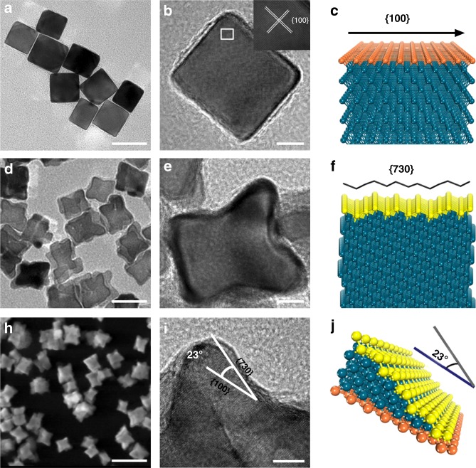
Fig. 1.
Characterization of the as-fabricated Pd nanocrystals. a TEM image of Pd nanocubes (Pd NCs) enclosed by {100} surface facets. Scale bar: 50 nm. b TEM image of a single Pd NC. Scale bar: 10 nm. c Atomic configuration diagram of Pd NCs. d TEM image of Pd concave nanocubes (Pd CNCs) enclosed by {730} surface facets. Scale bar: 50 nm. e TEM images of a single Pd CNC. Scale bar: 10 nm. f Atomic configuration diagram of Pd CNCs. g HAADF-STEM image of Pd CNCs. Scale bar: 100 nm. h High resolution TEM (HRTEM) image of Pd CNCs. Scale bar: 5 nm. i Model of the atomic arrangement on the {730} surface

