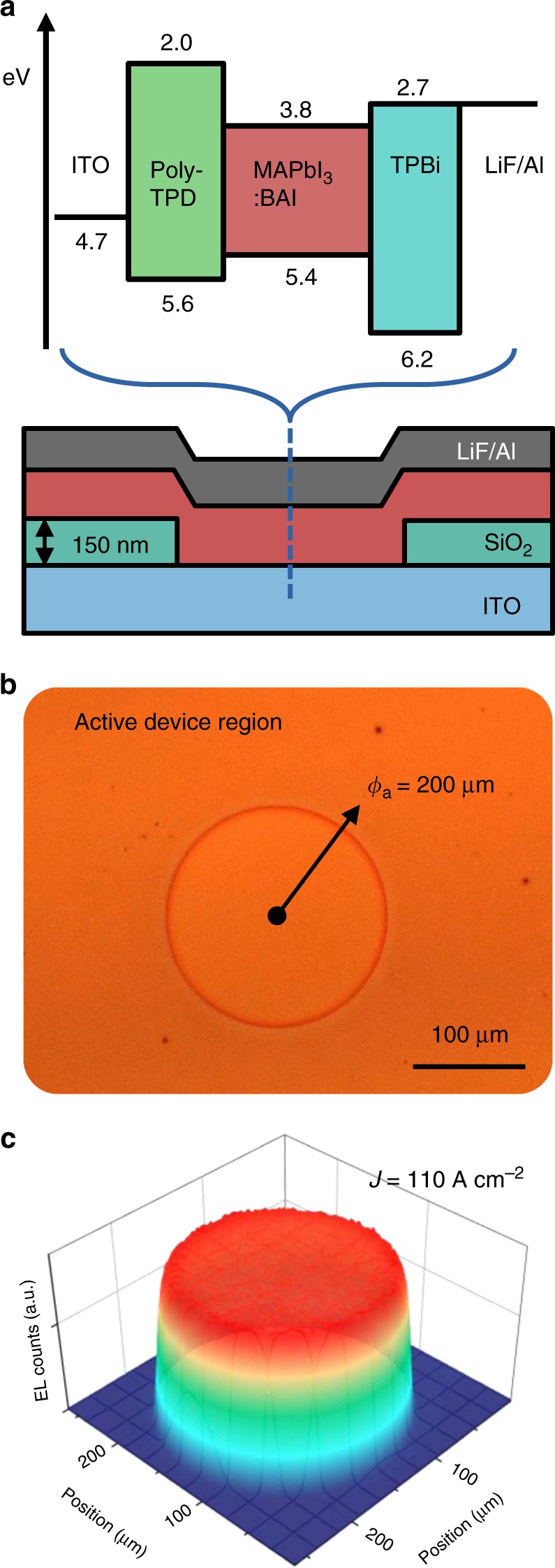
Fig. 1.

Device architecture. a Energy level diagram and schematic of the device architecture, which consists of ITO (150 nm)/poly-TPD (25 nm)/MAPbI3:BAI (100:20, 70 nm)/TPBi (40 nm)/LiF (1.2 nm)/Al (100 nm). The active area is defined by patterning openings in the insulating SiO2 (150 nm) layer shown in the bottom graphic. b Optical microscope image of a typical 200 μm diameter device. c Electroluminescence intensity profile recorded with the microscope camera, demonstrating uniform illumination even at a pulsed current density of 110 A cm−2
