Figure 8.

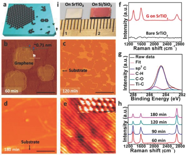
a) Schematic of graphene growth on STO (001) substrates. b–d) AFM images of the graphene grown by CVD technique for different duration. Scale bars: (b) 250 nm. (c,d) 1 µm. e) STM image (V s = 0.7 µV, I t = 18 nA) of a graphene film. Scale bar: 1 nm. Inset: STM image of graphene honeycomb lattice. Scale bar: 0.5 nm. f) Raman analysis of as‐grown graphene and bare STO substrates. g) XPS spectrum of as‐grown graphene. h) Raman analysis of graphene for the evolution of graphene growth. i) Photograph of an as‐grown graphene film on STO and a transferred graphene film to Si/SiO2 substrate. Reproduced with permission.63 Copyright 2014, American Chemical Society.
