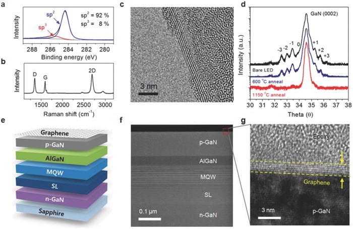
Figure 19.

a) XPS spectrum of the C 1s core level and b) Raman spectrum of a DG film synthesized for 3 h under a plasma power of 50 W. c) HRTEM image of the graphene edge on a TEM grid. d) HR‐XRD curves of the InGaN/GaN MQWs before and after thermal treatment. e) Schematic diagram and f) scanning TEM image of the DG/LED structure. g) HRTEM image at the interface between the p‐GaN and DG electrodes. Reproduced with permission.140 Copyright 2014, American Chemical Society.
