Fig. 1.
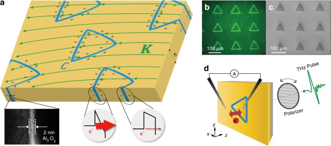
Ring-shaped quantum barriers. a An external current source generates a surface current (denoted by a vector field K) which applies a potential difference across the looped quantum barriers (denoted by contour C) laterally placed on a metallic plane. A TEM picture shows the cross-sectional image of the barrier which is composed of 2-nm-thick Al2O3 layer sandwiched in the gold film. Potentials on the barriers are very sensitive to the angle between the contour and the surface current K, reflected in the uneven charge density along each contour element. Electron tunneling probabilities through the barriers are critically affected by the potential difference. b An optical microscope image and c scanning electron microscope (SEM) image of fabricated triangle loops (side length of 70 μm, gap size of 2 nm). The contrast between the inside and outside of the loops in (c) indicates that the ring barriers are well-isolated electrically from the surroundings, affecting the electron emission density during the scanning. d Schematic of tunneling current measurement under THz field illumination. The THz field induces eddy currents on the sample surface, which acts as a current source K both inside and outside of the triangle as shown in (a). Incident polarization of the THz field is controlled by a THz polarizer. Tunneling current through the ring barrier is measured directly by electrical probes

