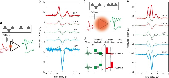
Fig. 6.
Experimental demonstration of ultrafast rectification. a Half-wave rectification. Demonstration of a half-rectifying barrier element (side length of 100 μm, gap size of 4 nm). A DC bias imposes potential difference for the contour element, giving a preferred current direction. THz tunneling current is thus rectified on one side of the triangle and an optical pulse selectively probes the temporal dynamics of the rectified current. A multi-cycle THz pulse is used to make a definite oscillating feature of the rectified pulse shape. b Demonstration of a half-rectifying barrier element (side length of 100 μm, gap size of 4 nm) for the THz pulses as a function of DC bias. c Full-wave rectification. To probe the total THz current, the optical spot is expanded to cover the entire loop. A multi-cycle THz pulse is used. d Schematic description of the time-dependent current response in a triangle barrier under a DC bias. The first column shows the specific time of the voltage pulse applied to the barrier, as indicated by black arrows. The second and third columns show the time-dependent potential V(l,t) and tunneling current density Jt(l,t) (Eq. 3 in Methods) as a function of arc length l (x-axis) defined in Fig. 2 (a) and time t (row). The final column shows the time-dependent total current direction (inward or outward from the loop). DC bias is described as grey bars and the offset lines in the potential distribution along the circumferential direction. e Demonstration of full-rectifying ring barriers (side length of 70 μm, gap size of 2 nm) as a function of DC bias. Dashed green curves in (b) and (e) show the THz voltage profile acquired from the incident THz pulse profile and Eq. (1). In panel (b) and (e), the value of the applied DC bias is denoted for each curve and the curves are vertically displaced for clarity

