Figure 6.

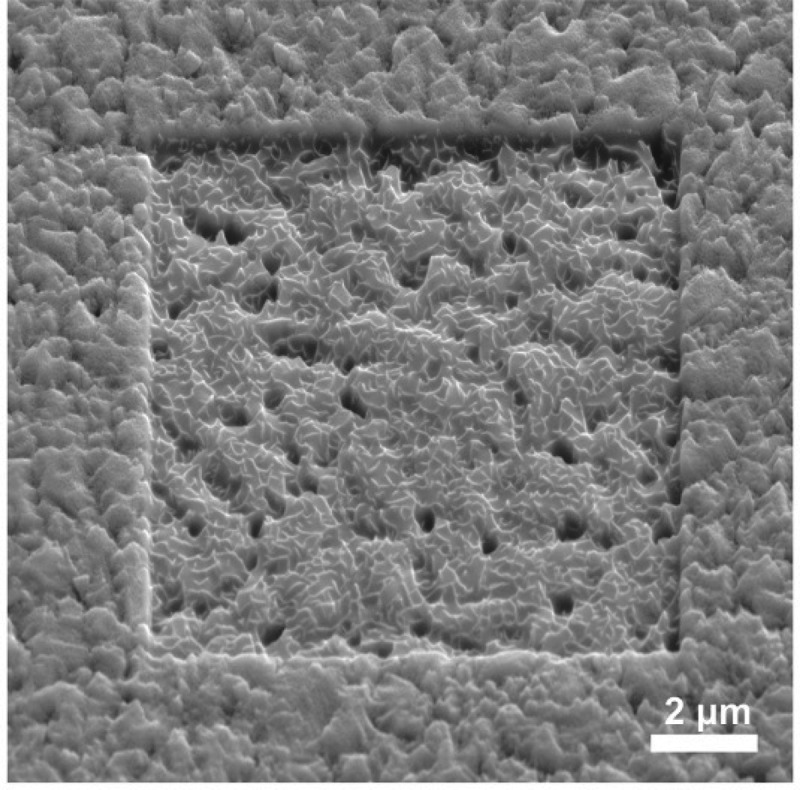
SEM micrograph of a completed CIGS sample surface (equivalent to Sample 3) after sputtering with Ga FIB on a 10 x 10 μm2 area (20 keV, 182 pA).

SEM micrograph of a completed CIGS sample surface (equivalent to Sample 3) after sputtering with Ga FIB on a 10 x 10 μm2 area (20 keV, 182 pA).