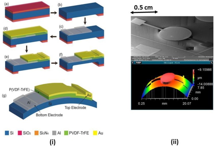
Figure 15.
(i) Steps to fabricate ultra-thin silicon based PVDF-TrFE capacitors: (a) Hard mask growth (b)Backside patterning to open etching window (c) Bottom metal deposition and patterning (d) PVDF-TrFE spin coating, annealing and top metal deposition (e) Patterning top metal and dry etching of polymer (f) Wet etching of bulk silicon (g) Final device on thin silicon (ii) (top) Scanning Electron Microscopy image of the piezo-capacitor sensor (bottom) optical profilometer image showing warp image of thin chip with the piezo-capacitor. Reprinted with permission from [110] © 2016 Elsevier.

