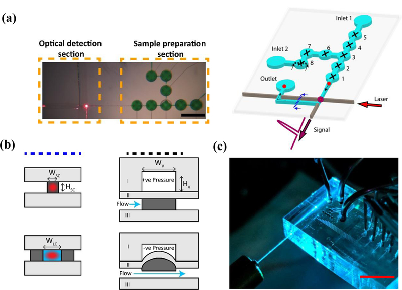
Figure 1: Schematic of the optofluidic device:

(a) (Left) A top-down image of the actual device with the two principal sections of the device shown (Scale bar: 1mm). (Right)The valves (1–8) are pneumatically controlled and individually programmable for operation. Samples are inserted through the inlets, and then captured and labelled with a fluorophore using the valves, before being pushed through to the optical section. The tagged particle (shown in red) is excited via laser coupled through the integrated PDMS waveguide (shown in brown) and the signal collected via an orthogonal liquid-core waveguide. The dotted lines indicate the cross sections shown in Figure 1(b). (b) Cross-sectional schematics of the sections in Figure 1(a) – operation of the optical waveguides and the pneumatic valves. Light grey indicates PDMS layer with 1:10 (curing agent: base) mixture, dark grey indicates layer PDMS layer with 1:5 (curing agent: base) mixture, blue indicates liquid volume and red indicates an excitation laser spot. The valves operate by applying positive pressure to keep the valve closed, or vacuum to open the valves. (c) A photograph of the actual chip (Scale bar: 1 cm) - the laser is coupled into the PDMS waveguides via a butt-coupled optical fiber, while metal tubings are used to provide access for pneumatic and fluidic control.
