Figure 1.
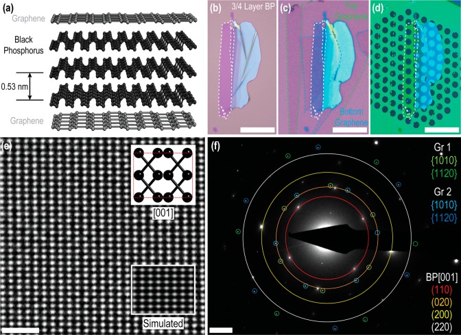
(a) Schematic of the graphene-encapsulated BP sample. (b) Optical micrograph of a 3–4 layer BP flake after exfoliation on an oxidized silicon substrate. (c) The same BP flake after top and bottom graphene encapsulation. The dashed lines highlight edges of mechanically exfoliated crystals. All exfoliation and transfer is performed in an argon environment glovebox to prevent oxidation of BP during the sample fabrication. (d) The same sample after transfer to a silicon nitride TEM support film. Scale bars for parts b–d are 20 μm. (e) Atomic-resolution Wiener-filtered aberration-corrected TEM image of a 5-layer thick area of pristine BP flake. The insets show an image simulation and ball-and-stick model of the [001] orientation. Scale bar is 1 nm. (f) Diffraction pattern from the area imaged in part e, showing two sets of spots corresponding to the upper and lower graphene sheets (misoriented by ∼20°), and the expected BP diffraction spots. The inner BP spots are forbidden reflections which are only visible in few-layered BP flakes (see Supporting Information, Figure S3, for diffraction pattern without overlays). Scale bar is 2 nm–1.

