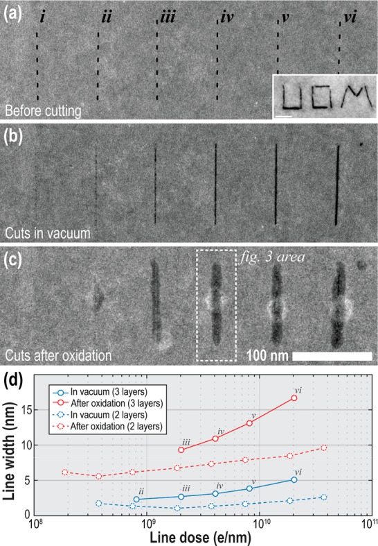
Figure 2.

HAADF STEM images showing the controlled cutting of nm-resolution lines in an encapsulated (3 layer) BP flake. The width of the 100 nm long cuts is controlled by varying dwell time per pixel (i) 0.05, (ii) 0.1, (iii) 0.25, (iv) 0.5, (v) 1, and (vi) 2.5 s. Lines were drawn using a probe current of 1.3 nA, an accelerating voltage of 200 kV and 1 pixel/nm. (a) shows the area immediately prior to patterning. (b) Cuts immediately after patterning. (c) Same cuts after exposing sample to air at room temperature for 2 days. (d) Solid lines are a comparison of line widths on initial sculpting in the electron microscope (blue data) and after oxidation in air (red data) taken from the area shown in parts a–c. The dashed lines show the change in line widths in a 2 layer sample as pictured in supporting material Figure S10. The inset in part a is a demonstration of electron beam writing of “UOM” into a 10 nm thick BP crystal (scale bar: 20 nm).
