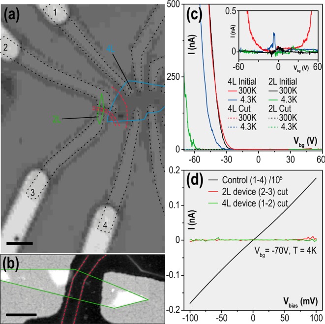
Figure 4.

Electrical characterization of patterned few layer BP. (a) Optical micrograph of the device with multiple metallic contacts highlighted by black dashed line. Blue line shows edges of 4 layer BP flake (4L) and green line 2 layer BP flake (2L). Red lines indicate etched lines (b) AFM topography of the 2L device with crystal edges highlighted with green. (c) Electrical current measured in a two terminal configuration (between contacts 1–2 for the 4L flake and 2–3 for the 2L flake) before and after the etching procedure. The inset shows the dotted traces (voltages after patterning) with a reduced vertical scale to enhance visibility. (d) Current voltage characteristics measured across the 2L and 4L devices compared to unetched 4L sample (contacts 1–4). Scale bars: (a) 2 μm and (b) 500 nm.
