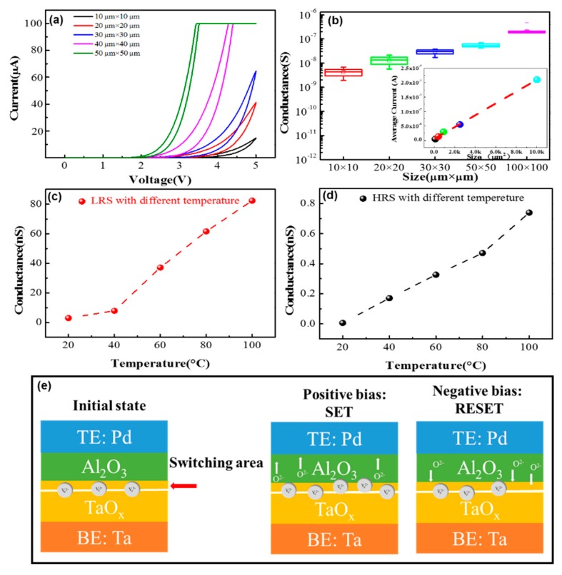
Figure 9.
(a) The I–V curves of the first SET process with different electrode area sizes (from 10 μm × 10 μm to 100 μm × 100 μm). (b) Conductance distribution at LRS with different sized areas (the conductance states are obtained by 1 V reading voltage in 25 different devices) (inset: the linear fit result confirms that the device conductance scales linearly with device areas). (c) Conductance of LRS with different temperatures from 20 to 100 °C; (d) Conductance of HRS with different temperatures from 20 to 100 °C. (e) The schematic of the switching mechanism of the device; the switching area is the interface of TaOx-Al2O3, and the push-and-pull of the oxygen ions in the surface can change the resistance of the interface layer.

