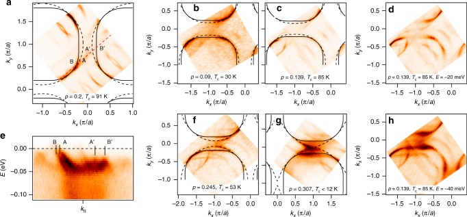
Fig. 1.
Development of the electronic structure of Bi2Sr2CaCu2O8+δ at the Fermi level with doping. a Fermi surface of an as grown sample. b, c Underdoped samples, obtained by annealing of the as grown samples in vacuum. f, g Overdoped samples, obtained by annealing of as grown samples in O3. Spectral intensity, represented by the false color contours, is integrated within ±2.5 meV around the Fermi level. Solid (dashed) lines represent the bonding (antibonding) states obtained from the tight-binding approximation that best fits the experimental data. The fitting involved the lines connecting the experimental minimal gap loci in all cases where the underlaying Fermi surface was gapped, as indicated in e. e Dispersion of states along the red dashed line in a. Fermi momenta of bonding (B, B′) and antibonding (A, A′) are marked in both a and e. Gapped Fermi momenta (A′, B′) were approximated by the points where the dispersion acquire maximum. d Intensity contour for sample UD85 (from c) at E = −20 meV and h E = −40 meV. The area enclosed by the TB lines that best represent the experimental data is calculated and used for determination of the doping parameter pA. The superconducting transition temperature, Tc, is determined from magnetic susceptibility measurements (as grown and underdoped samples) and from ARPES data, as explained in the text. All the maps were recorded at 12–20 K

