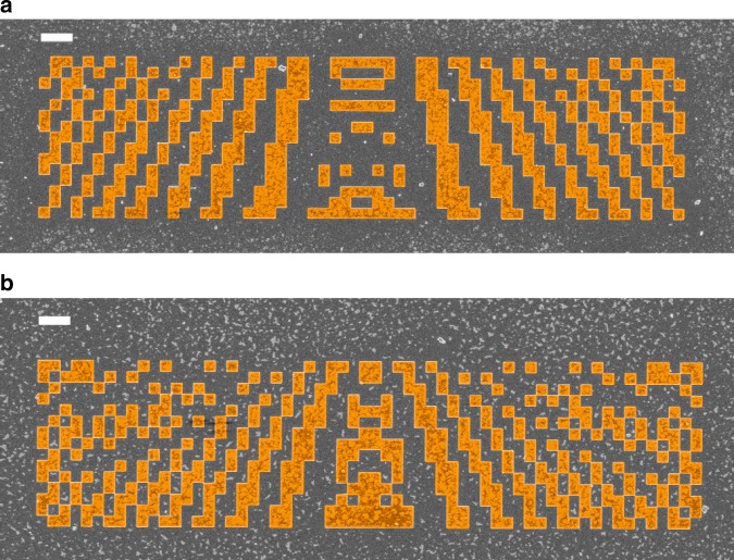
Fig. 3. SEM micrographs of the fabricated samples for the two elements on which we concentrate here, and the elements are highlighted in light brown.
a Element 1 serves the purpose of focusing the BSW 5 µm behind the element. b Element 2 serves the purpose of focusing the BSW directly behind the element with a focal width <0.5 λBSW. The spatial extent covered by the element is 40 µm by 10 µm, and each pixel of the checkerboard has a side length of 667 nm. The white scale bar indicates 2 µm. The applied conductive layer to enable SEM imaging on the dielectrics results in visible artifacts as tiny particles, but the layer is removed before the SNOM measurements

